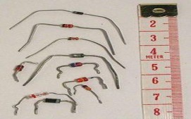
A diode is an electrical component acting as a one-way valve for current. The most common kind of diode in modern circuit design is the semiconductor diode, although other diode technologies exist. Semiconductor diodes are symbolized in schematic diagrams such as Figure below. The term “diode” is customarily reserved for small signal devices, I ≤ 1 A. The term rectifier is used for power devices, I > 1 A.
![]()
→ Semiconductor diode schematic symbol: Arrows indicate the direction of electron current flow.
When voltage is applied across a diode in such a way that the diode allows current, the diode is said to be forward-biased.
When voltage is applied across a diode in such a way that the diode prohibits current, the diode is said to be reverse-biased.
Có thể bạn quan tâm!
-
 Tiếng Anh chuyên ngành Nghề Điện tử công nghiệp - CĐ Công nghiệp và Thương mại - 7
 -
 Tiếng Anh chuyên ngành Nghề Điện tử công nghiệp - CĐ Công nghiệp và Thương mại - 8
 -
 Tiếng Anh chuyên ngành Nghề Điện tử công nghiệp - CĐ Công nghiệp và Thương mại - 9
 -
 Tiếng Anh chuyên ngành Nghề Điện tử công nghiệp - CĐ Công nghiệp và Thương mại - 11
 -
 Tiếng Anh chuyên ngành Nghề Điện tử công nghiệp - CĐ Công nghiệp và Thương mại - 12
 -
 Tiếng Anh chuyên ngành Nghề Điện tử công nghiệp - CĐ Công nghiệp và Thương mại - 13
Xem toàn bộ 134 trang tài liệu này.
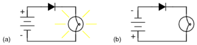
Diode operation: (a) Current flow is permitted; the diode is forward biased. (b) Current flow is prohibited; the diode is reverse biased.
Diode behavior is analogous to the behavior of a hydraulic device called a check valve. A check valve allows fluid flow through it in only one direction as in Figure below.
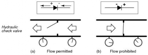
Hydraulic check valve analogy: (a) Electron current flow permitted. (b) Current flow prohibited.
Like check valves, diodes are essentially “pressure-” operated (voltage- operated) devices. The essential difference between forward-bias and reverse- bias is the polarity of the voltage dropped across the diode. Let's take a closer look at the simple battery-diode-lamp circuit shown earlier, this time investigating voltage drops across the various components in Figure below.
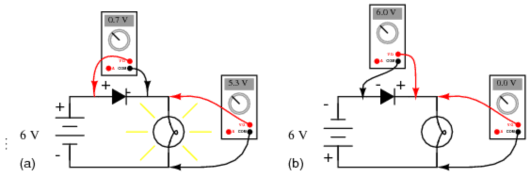
Diode circuit voltage measurements: (a) Forward biased. (b) Reverse biased.
The voltage dropped across a conducting, forward-biased diode is called the forward voltage. Forward voltage for a diode varies only slightly for changes in forward current and temperature, and is fixed by the chemical composition of the P-N junction.
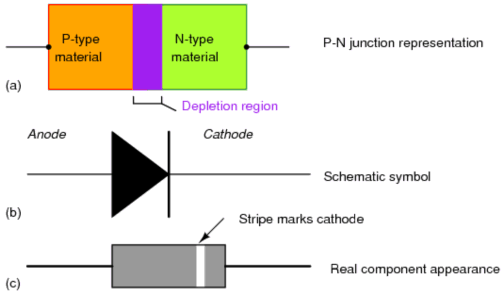
Diode representations: PN-junction model, schematic symbol, physical part.
The schematic symbol of the diode is shown in Figure above (b) such that the anode (pointing end) corresponds to the P-type semiconductor at (a). The cathode bar, non-pointing end, at (b) corresponds to the N-type material at (a). Also note that the cathode stripe on the physical part (c) corresponds to the cathode on the symbol.
If a reverse-biasing voltage is applied across the P-N junction, this depletion region expands, further resisting any current through it. (Figure below)
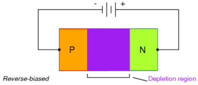
→ Depletion region expands with reverse bias.
Conversely, if a forward-biasing voltage is applied across the P-N junction, the depletion region collapses becoming thinner. The diode becomes less resistive to current through it. In order for a sustained current to go through the diode; though, the depletion region must be fully collapsed by the applied voltage. This takes a certain minimum voltage to accomplish, called the forward voltage as illustrated in Figure below.
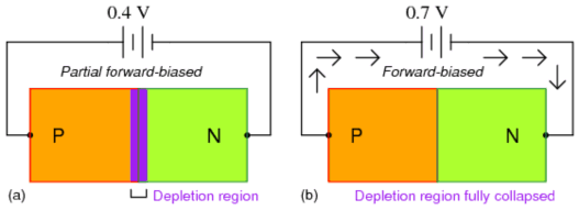
Increasing forward bias from (a) to (b) decreases depletion region thickness.
Silicon diodes have a forward voltage of approximately 0.7 volts.
Germanium diodes have a forward voltage of approximately 0.3 volts.
The maximum reverse-bias voltage that a diode can withstand without “breaking down” is called the Peak Inverse Voltage, or PIV rating.
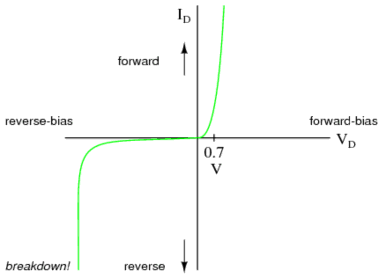
Diode curve: showing knee at 0.7 V forward bias for Si, and reverse breakdown.
Typically, the PIV rating of a generic “rectifier” diode is at least 50 volts at room temperature. Diodes with PIV ratings in the many thousands of volts are available for modest prices.
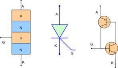
2. Thyristors
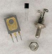
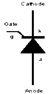
Common Thyristor Thyristor Circuit Symbol
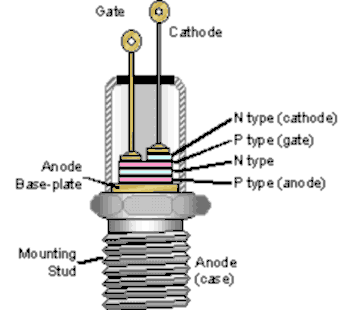
Typical Medium Power Thyristor Construction
To turn the thyristor off, the current flowing between anode and cathode must be reduced below a certain critical “holding current” value, (near to zero); alternatively the anode and cathode may be reverse biased.
The thyristor is normally made to conduct by applying a gating pulse, while the main anode and cathode terminals are forward biased. When the device is reverse biased, a gating pulse has no effect.
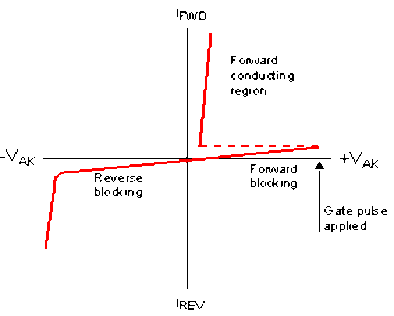
The fingure below shows a typical characteristic curve for a thyristor. It can be seen that in the reverse biased region it behaves in a similar way to a diode. All current, apart from a small leakage current is blocked (reverse blocking region) until the reverse breakdown region is reached, at which point the insulation due to the depletion layers at the junctions breaks down.
Typical Thyristor Characteristics
To understand the operation of a thyristor, think of it as a two-transistor (pnp and npn) model. If no gate signal is applied, but a voltage is applied (less than
forward breakdown voltage) between the top emitter terminal (marked A) and the bottom emitter terminal (marked K) so that A is positive with respect to K, both transistors will be turned off. No current is flowing so the voltage on the gate and cathode will be the same.
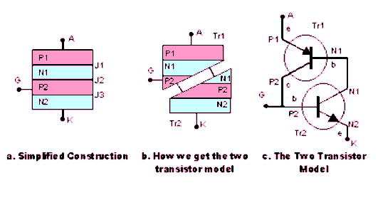
The Thyristor “Two Transistor Model”
When the gate is made positive with respect to K by the application of a gating pulse, Tr2 will turn on and its collector voltage will fall rapidly. This will cause the pnp transistor Tr1 base emitter junction to become forward biased, turning on Tr1. A large current will now be flowing between A and K. The action described happens very quickly as the switching on of Tr2 by Tr1 is a form of positive feedback with each transistor collector supplying large current changes to the base of the other.
As Tr1 collector is connected to Tr2 base, the action of switching on Tr1 connects Tr2 base virtually to the high positive voltage at A. This ensures that Tr2 ( and therefore Tr1) remains in conduction, even when the gating pulse is removed.
Because of the thyristor´s ability to switch very large currents at very high (hundreds of volts) voltages, the thyristor is a useful device in power control circuits. It is quite capable of handling AC mains and is used in such circuits as lighting dimmers, motor speed controls etc. They are also widely used as fast acting protection devices in DC power supplies. The switching speed of thyristors is very fast and they are able to switch from fully off to fully on, typically in 1µs.
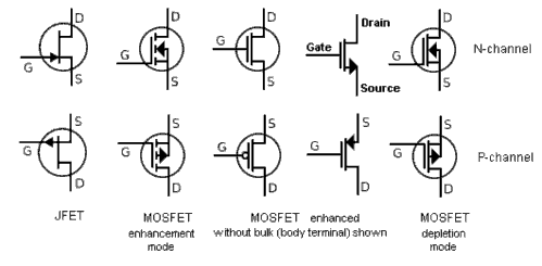
3. MOSFETS
Here are the symbols for FETs and MOSFETs:
Here is an animation showing how to turn on an N-channel MOSFET:
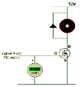
→ MOSFET turns ON when gate-to- source is more than about 2v (2v to 5v)
Here is a comparison between an NPN transistor and N-channel MOSFET:
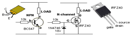
A zener must be added to the gate of a MOSFET if the gate voltage comes from a supply that is above 20v. A normal transistor is a current amplifying device. For a load current of 100mA, the base current for a BC547 will need to be about 1mA. This means it has a current gain of about 100.