ACKNOWLEDGEMENTS
I would like to sincerely thank the teachers of the Vietnam - Korea Friendship Information Technology College, who directly taught and imparted useful knowledge to me, which are the basic foundations, the extremely valuable provisions, the first step for me to enter my future career. Especially Ms. Tran Thi Tra Vinh has wholeheartedly helped me throughout the internship until the completion of the graduation project, answering questions during the implementation process. Thanks to that, I was able to complete this graduation project.
During the project, due to limited time, the graduation report will inevitably have errors. I sincerely hope to receive comments from teachers and friends so that my knowledge can be increasingly improved and I can draw useful experiences that can be effectively applied in practice in the future.
I wish you always happy, healthy and successful in your work.
Thank you very much.
Da Nang, May 2016
Le Tan Vang
INDEX
THANK YOU i
TABLE OF CONTENTS ii
LIST OF ABBREVIATIONS v
LIST OF DRAWINGS vii
LIST OF TABLES ix
INTRODUCTION 1
CHAPTER 1 OVERVIEW OF GSM NETWORK AND SMS MESSAGING SERVICE 2
1.1. OVERVIEW OF GSM MOBILE INFORMATION SYSTEM 2
1.1.1. Introduction to GSM mobile communication system 2
1.1.2 Characteristics of GSM mobile communication system 2
1.1.3 Structure of GSM mobile communication system 3
1.1.3.1 General structure 3
1.1.3.2 Components of GSM mobile communication system 3
1.1.4 Development of mobile information systems in Vietnam 4
1.2. OVERVIEW OF SMS MESSAGES 4
1.2.1 Introduction to SMS 4
1.2.2 Structure of an SMS message 6
1.2.3 SMS Message Sequence 7
1.2.4 SMS CENTER/SMSC 7
1.2.5 International SMS Messaging 8
CHAPTER 2 PIC16F887 MICROCONTROLLER 9
2.1. INTRODUCTION TO PIC (Programmable Intelligent Computer) 9
2.1.1. Introduction to PIC 9 microcontroller
2.1.2. Advantages and disadvantages of PIC 10
2.2 GENERAL INTRODUCTION TO PIC16F887 10
2.2.1 Introduction to PIC16F887 10
2.2.2 Block diagram of PIC16F887 12
2.3 SURVEY OF PIN DIAGRAM, FUNCTION OF EACH PIN 13
2.3.1 PIC16F887 microcontroller pin diagram 13
2.3.2 Memory organization 15
2.3.2.1 Program memory 15
2.3.2.2 Data memory 17
2.3.3 I/O ports of PIC16F887 17
2.4 ANALOG-DIGITAL CONVERTER (ADC) 19
2.4.1 AD 20 conversion result
2.4.2 Analog-to-digital conversion steps 21
2.4.3 ADC registers 22
2.5 COMPARATOR 22
2.6 EUART 24 SERIAL COMMUNICATION
2.6.1 The EUSART operates in asynchronous mode 24
2.6.1.1 EUSART 25 Asynchronous Transmitter
2.6.1.2 EUSART 26 Asynchronous Receiver
2.6.1.3 Clock accuracy with asynchronous operation 28
2.6.2 The EUSART operates in synchronous mode 30
2.7 TIMER 30 OPERATION
2.7.1 TIMER0 30 timer
2.7.2 TIMER1 32
2.7.3 TIMER2 34
2.8 INTERRUPT 35
CHAPTER 3 DESIGNING A CIRCUIT TO AUTOMATICALLY BALANCE TEMPERATURE AND CONTROL DEVICES VIA SMS MESSAGES 37
3.1 INTRODUCTION TO SIM900A MODULE, AT COMMAND SET. 37
3.1.1 Introduction to SIM900A module 37
3.1.2 Features of SIM900A module 37
3.1.3 Examine the pin diagram and function of each pin 40
3.1.4 Survey of AT command set of SIM900A module 42
3.2 SYSTEM BUILDING 44
3.2.1 Automatic temperature balance section 44
3.2.2 SMS control section 45
3.3 HARDWARE DESIGN 46
3.3.1 Circuit diagram 46
3.3.1.1 Source 46
3.3.1.2 Thermal balance circuit 46
3.3.1.3 Control circuit 47
3.3.1.4 Relay 47
3.3.3 Layout circuit 48
CHAPTER 4. RESULTS ACHIEVED BY THE SYSTEM 50
4.1 RESULTS ACHIEVED 50
4.2 PRODUCT OPERATION PROCESS 50
CONCLUSION 53
REFERENCES x
APPENDIX xi
LIST OF ABBREVIATIONS
Written Words
turn off
English Terminology | Vietnamese terminology | |
3GPP | Third Generation Partnership Project | Third-party collaboration projects |
ADC | Analog Digital Converter | Signal converter from analog to digital |
AUC | Authentication Center | Authentication Center |
BSS | Base Station Subsystem | Sub-base station system |
BTS | Base Transceiver Station | Base Transceiver Station. |
CDMA | Code Division Multiple Access | Code division multiple access |
CSPDN | Circuit Switched Public Data Network | Public data network channel circuit |
EDGE | Enhanced Data Rates for Global Evolution | Increase data transmission speed |
EIR | Equipment Identity Register | Device identification logger. |
ETSI | European Telecommunications Standards Institute | Telecommunications Standards Institute Europe |
GPRS | General Packet Radio Service | General Packet Radio Service |
GSM | Global System for Mobile Communications | Digital Mobile Information System global |
HLR | Home Location Register | Place of permanent registration |
ISDN | Integrated Services Digital network | Integrated Services Digital Network. |
MS | Mobile Station | Mobile station |
MSC | Mobile-services Switching Centerr | Switching center network service |
NSS | Network Switching Subsystem | System switching network child |
OMC | Operation and Maintenance Center | Exploitation and maintenance center nourish |
OSS | Operation Subsystem | Subsystem operations |
PIC | Programmable Interface Controller | Programming control interface |
Maybe you are interested!
-
 Car body electrical practice - 8
zt2i3t4l5ee
zt2a3gs
zt2a3ge
zc2o3n4t5e6n7ts
If the voltage is out of specification, replace the wire or connector.
If the voltage is within specification, install the front fog light relay and follow step 5.
Step 5 Check the front fog light switch
- Remove the D4 connector of the fog light switch
- Use a multimeter to measure the resistance of the front fog light switch.
Measurement location
Condition
Standard
D4-3 (BFG) -D4-4 (LFG)
Light switchFront Fog OFF
>10kΩ
D4-3 (BFG) -D4-4 (LFG)
Front fog light switchON
<1 Ω
- Standard resistor
D4 connector is located on the combination switch assembly.
If the resistance is out of specification, replace the combination switch (the fog light switch is located in the combination switch).
If the resistance is within specification, follow step 6.
Step 6 Check wiring and connectors (front fog light relay-light selector switch)
- Disconnect connector D4 of the combination switch assembly
- Use a voltmeter to measure the voltage value of jack D4 on the wire side.
Measurement location
Control modecontrol
Standard
D4-3 (BFG) - (-) AQ
TAIL
11 to 14 V
D4 connector for the wiring of the combination switch assembly
If the voltage does not meet the standard, replace the wire or connector.
If the voltage is within standard, there may have been an error in the previous measurements.
Step 7 Check the front fog lights
- Remove the front fog light electrical connector.
- Supply battery voltage to the fog lamp terminals
Jack 8, B9 of front fog lamp on the electrical side
blind first.
Power supply location
Terms and Conditions
Battery positive terminal - Terminal 2Battery negative terminal - Terminal 1
Fog lightsbefore morning
- If the light does not come on, replace the bulb.
If the light is on, re-plug the jack and continue to step 8.
Step 8 Check wiring and connectors (relay and front fog lights)
- Disconnect the B8 and B9 connectors of the front fog lights.
- Use a voltmeter to measure voltage at the following locations:
Measurement location
Switch location
Terms and Conditions
B8-2 - (-) AQ
Electric lock ON TAIL size switchFog switch ON
11 to 14 V
B9-2 - (-) AQ
Electric lock ONTAIL size switch Fog switch ON
11 to 14 V
B8 and B9 connectors on the front fog lamp wiring side
Voltage is not up to standard, repair or replace the jack. If up to standard, there may have been an error in the measurement process.
2.2.4. Procedure for removing, installing and adjusting fog lights 1. Procedure for removing
- Remove the front inner ear pads
Use a screwdriver to remove the 3 screws and remove the front part of the front inner ear liner
-Remove the fog light assembly
+ Disconnect the connector.
+ Use a screwdriver to remove 3 screws to remove the fog light cover
2. Installation sequence
-Rotate the fog lamp bulb in the direction indicated by the arrow as shown in the figure and remove the fog lamp from the fog lamp assembly.
-Rotate the fog light bulb in the direction indicated by the arrow as shown in the figure and install the light into the fog light assembly.
- Use a screwdriver to install the fog light cover
-Install the electrical connector
Attention: Be careful not to damage the plastic thread on the lamp assembly.
- Install the front inner ear pads
Use a screwdriver to install the front inner bumper with 3 screws.
3. Prepare the vehicle to adjust the fog light convergence. Prepare the vehicle:
- Make sure there is no damage or deformation to the vehicle body around the fog lights.
- Add fuel to the fuel tank
- Add oil to standard level.
- Add engine coolant to standard level.
- Inflate the tire to standard pressure.
- Place spare tire, tools and jack in original design position
- Do not leave any load in the luggage compartment.
- Let a person weighing about 75 kg sit in the driver's seat.
4. Prepare to check the fog light convergence
a/ Prepare the vehicle status as follows:
- Place the car in a dark enough place to see the lines. The lines are the dividing line, below which the light from the fog lights can be seen but above which it cannot.
- Place the car perpendicular to the wall.
- Keep a distance of 7.62 m between the center of the fog lamp and the wall.
- Park the car on level ground.
- Press the car down a few times to stabilize the suspension.
Note: A distance of approximately 7.62 m is required between the vehicle (fog lamp center) and the wall to adjust the convergence correctly. If the distance of 7.62 m cannot be achieved, set the correct distance of 3 m to check and adjust the fog lamp convergence. (Since the target area varies with the distance, please follow the instructions as shown in the figure.)
b/ Prepare a piece of thick white paper about 2 m high and 4 m wide to use as a screen.
c/ Draw a vertical line through the center of the screen (line V).
d/ Set the screen as shown in the picture. Note:
- Keep the screen perpendicular to the ground.
- Align the V line on the screen with the center of the vehicle.
e/Draw the reference lines (H, V LH and V RH lines) on the screen as shown in the figure.HINT:
Mark the center of the fog lamp on the screen. If the center mark cannot be seen on the fog lamp, use the center of the fog lamp or the manufacturer's name mark on the fog lamp as the center mark.
H line (fog light height):
Draw a line across the screen so that it passes through the center mark. Line H should be at the same height as the center mark of the fog light bulb.
Line V LH, V RH (center mark position of left fog lamp LH and right fog lamp RH):
Draw two lines so that they intersect line H at the center marks.
5. Check the fog light convergence
a/ Cover the fog lamp or remove the connector of the other side fog lamp to prevent light from the unchecked fog lamp from affecting the fog lamp convergence test.
b/ Start the engine.
c/ Turn on the fog lights and make sure that the dividing line is outside the standard area as shown in the drawing.
6. Adjust the fog light convergence
Use a screwdriver to adjust the fog light to the standard area by turning the toe adjustment screw.
Note: If the screw is adjusted too far, loosen it and then tighten it again, so that the last rotation of the light adjustment screw is clockwise.
3. Self-study questions
1. Describe the operating principle of the lighting system with automatic headlight function
2. Describe the operating principle of the lighting system with the function of rotating headlights when turning
3. Draw diagram and connect lighting system on Hyundai Porter car
4. Draw diagram and connect lighting system on Honda Accord 1992
5. Draw the lighting circuit on a 1993 Toyota Lexus
LESSON 3 MAINTENANCE AND REPAIR OF SIGNAL SYSTEM
I. IMPLEMENTATION GOAL
After completing this lesson, students will be able to:
- Distinguish between types of signals on cars
- Correctly describe common symptoms and suspected areas causing damage.
- Connecting signal circuits ensures technical requirements
- Disassemble, install, check, maintain and repair the signal system to ensure technical requirements.
- Ensure safety in work and industrial hygiene
II. LESSON CONTENT
1. General description
The signal system equipped on cars aims to create signals to notify other vehicles participating in traffic about the vehicle's operating status such as: stopping, parking, braking, reversing, turning...
Signals are used either by light such as headlamps, brake lights, turn signals….. or by sound such as horns, reverse music….
Just like the lighting system. A signal system circuit usually consists of: battery, fuse, wire, relay, electrical load and control switch. Only some switches of the signal system are on the combination switch. The switches of other signals are usually located in different locations such as in the gearbox or brake pedal……
2. Maintenance and repair
2.1. Turn signals and hazard lights
The installation location of the turn signal is shown in Figure 3.1. The turn signal control switch is located in the combination switch under the steering wheel. Turning this switch to the right or left will make the turn signal turn right or left.
The hazard light switch is used when the vehicle has a problem while participating in traffic. When the hazard light switch is turned on, all the turn signals on the vehicle will light up at a certain frequency. The hazard light switch is usually placed separately from the turn signal switch (some old cars integrate the hazard and turn signal switches on the same combination switch cluster).
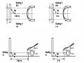
Figure 3.1 Turn signal switch Figure 3.2 Hazard switch
The part that generates the flashing frequency for the lights is called a turn signal relay. The turn signal relay usually has 3 terminals: B (positive power supply); E (negative power supply); L (providing the turn signal switch to distribute to the
lamp)
2.1.1. Circuit diagram
To generate the frequency for the turn signal, a turn signal relay is used in the turn signal circuit. The current from the turn signal relay will be sent to the turn signal switch assembly to distribute the current to the turn signal lights for the driver's purpose.
Figure 3.3. Schematic diagram of a turn signal circuit without a hazard switch
1. Battery; 2. Electric lock; 3. Turn signal relay; 4. Turn signal switch; 5. Turn signal lamp; 6. Turn signal lamp; 7. Hazard switch
Figure 3.4 Schematic diagram of turn signal circuit with hazard switch
1. Battery; 2. Combination switch cluster; 3. Turn signal;
4. Turn signal light; 5. Turn signal relay
Today's cars no longer use three-pin turn signal relays (B, L, E) but use eight-pin turn signal relays (figure 3.5) (pin number 8 is used for hazard lights).
For this type, the current supplying the turn signal lights is supplied directly from the turn signal relay to the lights.
div.maincontent .p { color: black; font-family:"Times New Roman", serif; font-style: normal; font-weight: normal; text-decoration: none; font-size: 14pt; margin:0pt; } div.maincontent p { color: black; font-family:"Times New Roman", serif; font-style: normal; font-weight: normal; text-decoration: none; font-size: 14pt; margin:0pt; } div.maincontent .s1 { color: black; font-family:"Times New Roman", serif; font-style: normal; font-weight: normal; text-decoration: none; font-size: 13pt; } div.maincontent .s2 { color: black; font-family:"Times New Roman", serif; font-style: italic; font-weight: normal; text-decoration: none; font-size: 14pt; } div.maincontent .s3 { color: black; font-family:"Times New Roman", serif; font-style: normal; font-weight: normal; text-decoration: none; font-size: 14pt; } div.maincontent .s4 { color: black; font-family:"Times New Roman", serif; font-style: normal; font-weight: normal; text-decoration: none; font-size: 13pt; } div.maincontent .s5 { color: black; font-family:"Times New Roman", serif; font-style: normal; font-weight: normal; text-decoration: none; font-size: 13pt; vertical-align: 1pt; } div.maincontent .s6 { color: black; font-family:"Times New Roman", serif; font-style: normal; font-weight: normal; text-decoration: none; font-size: 11pt; } div.maincontent .s7 { color: black; font-family:"Times New Roman", serif; font-style: normal; font-weight: normal; text-decoration: none; font-size: 14pt; vertical-align: -9pt; } div.maincontent .s8 { color: black; font-family:"Times New Roman", serif; font-style: normal; font-weight: normal; text-decoration: none; font-size: 11pt; } div.maincontent .s9 { color: #008000; font-family:"Times New Roman", serif; font-style: normal; font-weight: normal; text-decoration: none; font-size: 14pt; } div.maincontent .s10 { color: black; font-family:"Times New Roman", serif; font-style: italic; font-weight: normal; te
Car body electrical practice - 8
zt2i3t4l5ee
zt2a3gs
zt2a3ge
zc2o3n4t5e6n7ts
If the voltage is out of specification, replace the wire or connector.
If the voltage is within specification, install the front fog light relay and follow step 5.
Step 5 Check the front fog light switch
- Remove the D4 connector of the fog light switch
- Use a multimeter to measure the resistance of the front fog light switch.
Measurement location
Condition
Standard
D4-3 (BFG) -D4-4 (LFG)
Light switchFront Fog OFF
>10kΩ
D4-3 (BFG) -D4-4 (LFG)
Front fog light switchON
<1 Ω
- Standard resistor
D4 connector is located on the combination switch assembly.
If the resistance is out of specification, replace the combination switch (the fog light switch is located in the combination switch).
If the resistance is within specification, follow step 6.
Step 6 Check wiring and connectors (front fog light relay-light selector switch)
- Disconnect connector D4 of the combination switch assembly
- Use a voltmeter to measure the voltage value of jack D4 on the wire side.
Measurement location
Control modecontrol
Standard
D4-3 (BFG) - (-) AQ
TAIL
11 to 14 V
D4 connector for the wiring of the combination switch assembly
If the voltage does not meet the standard, replace the wire or connector.
If the voltage is within standard, there may have been an error in the previous measurements.
Step 7 Check the front fog lights
- Remove the front fog light electrical connector.
- Supply battery voltage to the fog lamp terminals
Jack 8, B9 of front fog lamp on the electrical side
blind first.
Power supply location
Terms and Conditions
Battery positive terminal - Terminal 2Battery negative terminal - Terminal 1
Fog lightsbefore morning
- If the light does not come on, replace the bulb.
If the light is on, re-plug the jack and continue to step 8.
Step 8 Check wiring and connectors (relay and front fog lights)
- Disconnect the B8 and B9 connectors of the front fog lights.
- Use a voltmeter to measure voltage at the following locations:
Measurement location
Switch location
Terms and Conditions
B8-2 - (-) AQ
Electric lock ON TAIL size switchFog switch ON
11 to 14 V
B9-2 - (-) AQ
Electric lock ONTAIL size switch Fog switch ON
11 to 14 V
B8 and B9 connectors on the front fog lamp wiring side
Voltage is not up to standard, repair or replace the jack. If up to standard, there may have been an error in the measurement process.
2.2.4. Procedure for removing, installing and adjusting fog lights 1. Procedure for removing
- Remove the front inner ear pads
Use a screwdriver to remove the 3 screws and remove the front part of the front inner ear liner
-Remove the fog light assembly
+ Disconnect the connector.
+ Use a screwdriver to remove 3 screws to remove the fog light cover
2. Installation sequence
-Rotate the fog lamp bulb in the direction indicated by the arrow as shown in the figure and remove the fog lamp from the fog lamp assembly.
-Rotate the fog light bulb in the direction indicated by the arrow as shown in the figure and install the light into the fog light assembly.
- Use a screwdriver to install the fog light cover
-Install the electrical connector
Attention: Be careful not to damage the plastic thread on the lamp assembly.
- Install the front inner ear pads
Use a screwdriver to install the front inner bumper with 3 screws.
3. Prepare the vehicle to adjust the fog light convergence. Prepare the vehicle:
- Make sure there is no damage or deformation to the vehicle body around the fog lights.
- Add fuel to the fuel tank
- Add oil to standard level.
- Add engine coolant to standard level.
- Inflate the tire to standard pressure.
- Place spare tire, tools and jack in original design position
- Do not leave any load in the luggage compartment.
- Let a person weighing about 75 kg sit in the driver's seat.
4. Prepare to check the fog light convergence
a/ Prepare the vehicle status as follows:
- Place the car in a dark enough place to see the lines. The lines are the dividing line, below which the light from the fog lights can be seen but above which it cannot.
- Place the car perpendicular to the wall.
- Keep a distance of 7.62 m between the center of the fog lamp and the wall.
- Park the car on level ground.
- Press the car down a few times to stabilize the suspension.
Note: A distance of approximately 7.62 m is required between the vehicle (fog lamp center) and the wall to adjust the convergence correctly. If the distance of 7.62 m cannot be achieved, set the correct distance of 3 m to check and adjust the fog lamp convergence. (Since the target area varies with the distance, please follow the instructions as shown in the figure.)
b/ Prepare a piece of thick white paper about 2 m high and 4 m wide to use as a screen.
c/ Draw a vertical line through the center of the screen (line V).
d/ Set the screen as shown in the picture. Note:
- Keep the screen perpendicular to the ground.
- Align the V line on the screen with the center of the vehicle.
e/Draw the reference lines (H, V LH and V RH lines) on the screen as shown in the figure.HINT:
Mark the center of the fog lamp on the screen. If the center mark cannot be seen on the fog lamp, use the center of the fog lamp or the manufacturer's name mark on the fog lamp as the center mark.
H line (fog light height):
Draw a line across the screen so that it passes through the center mark. Line H should be at the same height as the center mark of the fog light bulb.
Line V LH, V RH (center mark position of left fog lamp LH and right fog lamp RH):
Draw two lines so that they intersect line H at the center marks.
5. Check the fog light convergence
a/ Cover the fog lamp or remove the connector of the other side fog lamp to prevent light from the unchecked fog lamp from affecting the fog lamp convergence test.
b/ Start the engine.
c/ Turn on the fog lights and make sure that the dividing line is outside the standard area as shown in the drawing.
6. Adjust the fog light convergence
Use a screwdriver to adjust the fog light to the standard area by turning the toe adjustment screw.
Note: If the screw is adjusted too far, loosen it and then tighten it again, so that the last rotation of the light adjustment screw is clockwise.
3. Self-study questions
1. Describe the operating principle of the lighting system with automatic headlight function
2. Describe the operating principle of the lighting system with the function of rotating headlights when turning
3. Draw diagram and connect lighting system on Hyundai Porter car
4. Draw diagram and connect lighting system on Honda Accord 1992
5. Draw the lighting circuit on a 1993 Toyota Lexus
LESSON 3 MAINTENANCE AND REPAIR OF SIGNAL SYSTEM
I. IMPLEMENTATION GOAL
After completing this lesson, students will be able to:
- Distinguish between types of signals on cars
- Correctly describe common symptoms and suspected areas causing damage.
- Connecting signal circuits ensures technical requirements
- Disassemble, install, check, maintain and repair the signal system to ensure technical requirements.
- Ensure safety in work and industrial hygiene
II. LESSON CONTENT
1. General description
The signal system equipped on cars aims to create signals to notify other vehicles participating in traffic about the vehicle's operating status such as: stopping, parking, braking, reversing, turning...
Signals are used either by light such as headlamps, brake lights, turn signals….. or by sound such as horns, reverse music….
Just like the lighting system. A signal system circuit usually consists of: battery, fuse, wire, relay, electrical load and control switch. Only some switches of the signal system are on the combination switch. The switches of other signals are usually located in different locations such as in the gearbox or brake pedal……
2. Maintenance and repair
2.1. Turn signals and hazard lights
The installation location of the turn signal is shown in Figure 3.1. The turn signal control switch is located in the combination switch under the steering wheel. Turning this switch to the right or left will make the turn signal turn right or left.
The hazard light switch is used when the vehicle has a problem while participating in traffic. When the hazard light switch is turned on, all the turn signals on the vehicle will light up at a certain frequency. The hazard light switch is usually placed separately from the turn signal switch (some old cars integrate the hazard and turn signal switches on the same combination switch cluster).
Figure 3.1 Turn signal switch Figure 3.2 Hazard switch
The part that generates the flashing frequency for the lights is called a turn signal relay. The turn signal relay usually has 3 terminals: B (positive power supply); E (negative power supply); L (providing the turn signal switch to distribute to the
lamp)
2.1.1. Circuit diagram
To generate the frequency for the turn signal, a turn signal relay is used in the turn signal circuit. The current from the turn signal relay will be sent to the turn signal switch assembly to distribute the current to the turn signal lights for the driver's purpose.
Figure 3.3. Schematic diagram of a turn signal circuit without a hazard switch
1. Battery; 2. Electric lock; 3. Turn signal relay; 4. Turn signal switch; 5. Turn signal lamp; 6. Turn signal lamp; 7. Hazard switch
Figure 3.4 Schematic diagram of turn signal circuit with hazard switch
1. Battery; 2. Combination switch cluster; 3. Turn signal;
4. Turn signal light; 5. Turn signal relay
Today's cars no longer use three-pin turn signal relays (B, L, E) but use eight-pin turn signal relays (figure 3.5) (pin number 8 is used for hazard lights).
For this type, the current supplying the turn signal lights is supplied directly from the turn signal relay to the lights.
div.maincontent .p { color: black; font-family:"Times New Roman", serif; font-style: normal; font-weight: normal; text-decoration: none; font-size: 14pt; margin:0pt; } div.maincontent p { color: black; font-family:"Times New Roman", serif; font-style: normal; font-weight: normal; text-decoration: none; font-size: 14pt; margin:0pt; } div.maincontent .s1 { color: black; font-family:"Times New Roman", serif; font-style: normal; font-weight: normal; text-decoration: none; font-size: 13pt; } div.maincontent .s2 { color: black; font-family:"Times New Roman", serif; font-style: italic; font-weight: normal; text-decoration: none; font-size: 14pt; } div.maincontent .s3 { color: black; font-family:"Times New Roman", serif; font-style: normal; font-weight: normal; text-decoration: none; font-size: 14pt; } div.maincontent .s4 { color: black; font-family:"Times New Roman", serif; font-style: normal; font-weight: normal; text-decoration: none; font-size: 13pt; } div.maincontent .s5 { color: black; font-family:"Times New Roman", serif; font-style: normal; font-weight: normal; text-decoration: none; font-size: 13pt; vertical-align: 1pt; } div.maincontent .s6 { color: black; font-family:"Times New Roman", serif; font-style: normal; font-weight: normal; text-decoration: none; font-size: 11pt; } div.maincontent .s7 { color: black; font-family:"Times New Roman", serif; font-style: normal; font-weight: normal; text-decoration: none; font-size: 14pt; vertical-align: -9pt; } div.maincontent .s8 { color: black; font-family:"Times New Roman", serif; font-style: normal; font-weight: normal; text-decoration: none; font-size: 11pt; } div.maincontent .s9 { color: #008000; font-family:"Times New Roman", serif; font-style: normal; font-weight: normal; text-decoration: none; font-size: 14pt; } div.maincontent .s10 { color: black; font-family:"Times New Roman", serif; font-style: italic; font-weight: normal; te -
 Voice Control Circuit Design - 7
 -
 Design and construction of color TV PAN model - 2
 -
 Building a system to monitor water level, temperature and send warnings via SMS/GSM network - 2
 -
 Network design - Master Tran Van Long, Master Tran Dinh Tung Compiled - 24
Public Land Mobile Network | Terrestrial mobile network. | |
PSP | Parallel Slave Port | Parallel Sub Port |
PSPDN | Packet Switch Public Data Network | Data switching network public |
PSTN | Public Switch Telephone Network | Public switched telephone network. |
PWM | Pulse Width Modulation | Voltage regulation method |
SIM | Subscriber Identity Module | Subscriber identification module |
SMS | Short Message Service | Short Message Service |
SMSC | Short message Service Center | Short Message Service Center |
SPI | Serial Peripheral Interface | Serial peripheral communication |
TDM | Time Division Multiplexing | Time division modulationspace |
TDMA | Time Division Multiple Access | Time division multiple access |
USB | Universal Serial Bus | Common serial port |
VLR | Visitor Location Register | Registration address |
WAP | Wireless Application Protocol | Application Protocol No wire |
PLMN
LIST OF DRAWINGS
Number
effect
Image name | Page | |
1.1 | Structure of GSM mobile communication system | 3 |
1.2 | GSM system components | 3 |
1.3 | Structure of an SMS message | 6 |
2.1 | PIC16F887 microcontroller block diagram | 12 |
2.2 | PIC16F887 microcontroller pin diagram | 13 |
2.3 | PIC16F887 program memory | 16 |
2.4 | Register address of PIC16F887 | 17 |
2.5 | Block diagram of AD | 20 |
2.6 | Clock cycle and operating frequency of ADC | 20 |
2.7 | Ways to save 10 bit A/D conversion results | 21 |
2.8 | Registers related to the A/D controller | 22 |
2.9 | Working principle of a simple comparator | 23 |
2.10 | Simple block diagram of Comparator | 23 |
2.11 | Registers related to the comparator | 24 |
2.12 | Block diagram of asynchronous EUSART data transmitter | 26 |
2.13 | Registers involved in asynchronous transmission | 26 |
2.14 | Block diagram of asynchronous EUSART data receiver | 27 |
2.15 | Registers involved in asynchronous data reception | 28 |
2.16 | TXSTA register structure | 28 |
2.17 | RCSTA register structure | 29 |
2.18 | Timer 0 timer block diagram | 31 |
2.19 | Registers related to Timer0 | 32 |
2.20 | T1CON: Timer1 control register | 33 |
2.21 | Timer1 block diagram | 33 |
2.22 | Registers related to Timer1 | 34 |
2.23 | T2CON: Timer2 control register | 35 |
2.24 | Block diagram of Timer2 timer | 35 |
Registers related to Timer2 | 35 | |
3.1 | SIM900A Module | 39 |
3.2 | SIM900A Module Pinout | 40 |
3.2 | Block diagram of self-balancing thermal system | 44 |
3.3 | Block diagram of device control system using SMS | 45 |
3.4 | Power circuit | 46 |
3.5 | Thermal balance circuit | 47 |
3.6 | Main control circuit | 47 |
3.7 | Relay | 48 |
3.8 | Temperature balance circuit | 48 |
3.9 | Main control circuit | 49 |
4.1 | Complete circuit | 50 |
4.2 | Turn on device 1 | 50 |
4.3 | Device 1 enabled notification | 50 |
4.4 | turn off device 1 | 51 |
4.5 | Device 1 turned off notification | 51 |
4.6 | Turn on device 2 | 51 |
4.7 | Device 2 enabled notification | 51 |
4.8 | Turn off device 2 | 51 |
4.9 | Device 2 turned off notification | 51 |
4.10 | Turn on device 3 | 51 |
4.11 | Device 3 enabled notification | 51 |
4.12 | Turn off device 3 | 52 |
4.14 | Turn on device 4 | 52 |
4.15 | Device 4 enabled notification | 52 |
4.16 | Turn off device 4 | 52 |
4.17 | Device 4 turned off notification | 52 |
4.18 | Check room temperature | 52 |
4.19 | Room temperature notification | 52 |
2.25