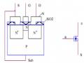
In the circuit where the external pulse only affects the conducting transistor, the two diodes D 1 and D 2 are biased by two resistors R 3 and R 4. In the saturated conducting transistor, Vc 0 V , so the reverse bias voltage for the diode is low, so when a negative pulse is applied, the diode is easily forward biased. In the non-conducting transistor, Vc = Vcc, so the reverse bias voltage for the diode is very high. Therefore, when the negative pulse arrives, it is not enough to forward bias the diode.
The R 3 C 1 and R 4 C 2 circuits are still considered to be differential circuits with a bias step that depends on the Vc of the transistor.
- To switch the circuit's working state well, the impact pulse must have an amplitude of polarity change and a time long enough for the transistor to switch to the working state.
- To make the circuit switch state well and work fast, you should choose a source with a low working voltage but still ensure the load requirements.
1.2. Phase shift oscillator circuit (Figure 5-14)
The main point is that the circuit is connected in common emitter mode. The feedback from the collector to the base is through the components C 1 , C 2 , C 3 , R 1 , R 2 , R 3 connected in series with the input. The resistor R 3 has the effect of changing the frequency of the oscillating circuit. For each RC phase shift circuit to create a phase shift of 60 0 then C 1 = C 2 = C 3 And R 1 = R 2 = R 3 . The frequency of the oscillating circuit fo is calculated:
1
f o =
2 . C . 6 R 2 .4 R . R
(5-11)
+
1 1 1 c
Rb1 Rc
C1 C2 C3
R3
R1 R2
Q
V o
Rb2
Vcc
Figure 5-14. Phase shift oscillator circuit
The circuit operates as follows: When powered through the voltage divider bridge Rb1 and Rb2 Q conducts electricity, the voltage on the C pole of the transistor Q decreases and is fed back through the feedback circuit C 1 , C 2 , C 3 and R 1 , R 2 , R 3 and is phase shifted by 180 0 so the amplitude increases in the same direction as the input (Positive feedback). The transistor continues to conduct strongly until it is saturated, then the capacitors discharge, causing the voltage at the B pole of the transistor to decrease, the transistor
switch to the stop state until the discharge is complete, the voltage at pole B increases to form a new conduction cycle. Forming a signal pulse at the output. The important point to remember is that the feedback loop must satisfy the condition that the phase of the output signal through the phase shift circuit must be 180 0. If this condition is not satisfied, the circuit cannot oscillate, or the output signal will be distorted asymmetrically.
The circuit is often used to generate pulses with adjustable frequencies such as longitudinal oscillator circuits in television technology. Because the circuit operates less stably when the power supply is unstable or the environmental humidity changes, it is rarely used in industrial electronics and devices that require high frequency stability.
1.3. Sine wave oscillation circuit
Sinusoidal oscillations have a wide range of applications in the electronics field, providing signal sources for electronic circuits during operation. There are many different types of sinusoidal oscillations, but all must contain the following two basic components:
- Frequency finder : It can be an LC resonant circuit or an RC circuit. The resonant circuit is a combination of inductor and capacitor, the frequency of the oscillating circuit is the frequency of the natural resonance of the LC circuit. The RC circuit does not naturally resonate but the phase shift of this circuit is used to determine the frequency of the oscillating circuit.
- Maintenance unit: has the task of providing additional energy to the resonator to maintain oscillation. This part itself must have a Vdc supply, usually an active component such as a transistor that conducts regular electrical pulses to the resonant circuit to supplement energy, must ensure phase shift and gain sufficient to compensate for the energy loss in the circuit.
1.3.1. LC oscillating circuit:
a. Three-point inductance oscillating circuit (Hartley) (Figure 5-15)
+V
T: Oscillating transformer
C1 Vo: think out
Rb
C2
Q
Figure 5-15. Three-point inductance sinusoidal oscillation circuit
On the circuit diagram connected in EC style, with the coil centered, the coil and capacitor C1 form a resonant frame that determines the oscillation frequency of the circuit. Capacitor C2 acts as a positive feedback signal to the base of the transistor to maintain oscillation. The circuit is biased by resistor Rb.
The feedback signal is taken on the arm of the inductor so it is called a three-point inductance oscillator circuit (hertlay).
b. Capacitive three-point oscillator circuit (Colpitts) (Figure 5-16)
+V
C3 Rb1
R c T: Oscillating transformer
C1
Vo: Sober up
C2
Q
Rb2
Figure 5-16. Three-point capacitive oscillator circuit
On the circuit diagram, it is connected in the EC style with the coil without a center point, the resonant frame consists of a coil connected in parallel with two capacitors C1, C2 connected in series, capacitor C3 acts as a positive feedback signal to the B pole of transistor Q to maintain oscillation, the circuit is polarized by the voltage divider bridge Rb1 and Rb2. The output signal is taken on the secondary coil of the oscillating transformer. In practice, to adjust the oscillation frequency of the circuit, people can adjust the narrow range by changing the B bias voltage of the transistor and adjust the large range by changing the inductance of the coil with a tuning core placed in the coil instead of a fixed core.
1.3.2. Quartz oscillator circuit (Figure 5-17)
Quartz is also known as piezoelectric ceramic, they have natural resonance frequency depending on the size and shape of the ceramic element used as a component, so they have a very high quality factor, narrow bandwidth, so the accuracy of the circuit is very high. Quartz oscillators are widely used in electronic devices with high frequency accuracy such as generating carrier waves of transmitters, clock pulses in microprocessor systems...
+V
Rb Rc
C1 Q
X
C2 Re
Vo: to wake up
Figure 5-17. Oscillator circuit using quartz The functions of the components in the circuit are as follows:
Q: oscillator transistor
R c : Load resistor to get output signal
Re : Temperature stabilizer and feedback signal
C 1 , C 2 : Voltage divider bridge uses capacitor to get feedback signal to pole BR b : Bias resistor B for transistor Q
X: quartz oscillator
+V: Power supply for the circuit
The circuit operates as follows: When the B bias voltage is supplied to the transistor Q, it simultaneously charges the crystal and two capacitors C1 and C2. This causes the voltage at pole B to decrease. When the circuit is fully charged, the voltage at pole B increases through the positive feedback loop C1, C2. The voltage at pole B continues to increase until the transistor conducts the signal to harmonize. The circuit begins to discharge through the BE junction of the transistor, causing the voltage at pole B of the transistor to decrease until the circuit is completely discharged, starting a new cycle of the signal. The frequency of the circuit is determined by the frequency of the crystal. The output signal is sinusoidal, so to create signals in the form of digital pulses for the control circuits, the pulse signals are sent to bistable multivibrator circuits (FF) to correct the signal shape.
2. Clipping circuit
Target:
- Draw and present the operating principles of clipping circuits using transistors.
- Present the applications of clipping circuits
The clipping circuit is also known as the signal clipping circuit, which aims to correct the shape and limit the signal amplitude, so it is very commonly used in control circuits and control signal processing. The clipping circuit can use Diodes or transistors and depending on the
Depending on the needs of the circuit, it can be trimmed above, trimmed below, or trimmed at two independent levels. In this article, only clipping circuits using transistors are introduced. The clipping level is established based on the bias mode of the transistor. (Figure 5-18)
saturation zone
IC
Q
IC
0 Vc
Vcc
amplification region
Ib
condensation zone
Uce
Figure 5-18. Transistor operating characteristics
Due to the working nature of the transistor, when the input signal amplitude of the circuit is below the working bias level, the transistor does not conduct, so the signal is clipped. Conversely, when the input signal exceeds the threshold level, the transistor is saturated and the signal is also clipped. Taking advantage of this nature, people design clipping circuits using transistors, including upper clipping circuits, lower clipping circuits, or clipping at two independent levels.
2.1. Upper and lower trim circuit
The circuit has the function of cutting off the upper or lower part of the input signal, often used to separate the individual signal in the common signal of many different signal components modulated in the form of amplitude or used to correct the signal shape, in this type of circuit, the transistor is statically polarized in mode AB, B, C, or D, tilted to the conduction region, depending on the signal level to be cut. (Figure 5-19) This is a circuit used to separate the synchronous signal in a mixed image signal in television technology with a positive phase input, the clipping circuit in this case is a lower level clipping circuit (cutting off the lower part of the signal).
V
Vc
+V
C2
V iRb
t
RC C1
Q V o
t
Input signal: Vi Output signal: Vo
Figure 5-19. Lower level clipping circuit
The circuit operates as follows: The statically biased transistor is located deep inside the condenser (Mode C) thanks to the resistor Rb biasing B to bring the transistor down to mass Vbe
=0v, the transistor stops conducting, the voltage at pole C = Vcc. When there is a positive phase input signal, the voltage at B gradually increases but is not large enough to make the transistor conduct until it reaches a large enough value, the transistor switches from the stopped state to the conducting state, quickly falls into the amplification region, the remaining signal amplitude is amplified and taken out on pole C. In the case of a negative phase input signal, the circuit has the opposite structure as shown in (Figure 5-20).
V
t
V
+V
Rb
C2 Q
C1
V o
V i t
Rc
Input signal: Vi Output signal: Vo
Figure 5-20. Upper level clipping circuit
In addition to the clipping circuit presented above, there are a number of other circuit types used to separate waves or generate pulses to stimulate control stages.
- The output is low frequency modulated signals.
- The signal has only one positive semi-cycle left.
signal cycle
- Input is high frequency modulated signals.
- The signal has two positive and negative half-cycles.
- Used in amplitude wave detector circuits in Radio
+V
Rb2
Rb1
C1
Q
Re Vo: think out
Figure 5-21. Subzero clipping circuit
In the circuit diagram (Figure 5-21), the BE junction of the transistor acts as a wave-cutting diode that cuts off the negative part of the signal (under-clipping) at zero volts, and at the same time acts as an amplifier circuit that amplifies the output signal current taken from the emitter (CC-connected circuit).
2.2. Clipping circuit at two independent levels
In this clipping circuit, depending on the needs of the circuit, people choose to clip two symmetrical or two unsymmetrical levels. An important issue in the clipping circuit using a transistor is that the input signal amplitude must be quite high to ensure that the clipped signal area is right in the cut-off or saturation region of the transistor, the output signal is in the amplification region. In the case of clipping two symmetrical independent levels, the transistor is biased in class A amplification mode. If clipping at two asymmetrical independent levels, depending on the requirements, people choose a PNP or NPN transistor and bias it in AB mode to increase the working life of the transistor.
- Symmetric clipping circuit, biased in gain mode A.
C3 Vi:Come in | Rb1 Rb2 | +V Rc Q | Vo: Sober up | - The output signal is clipped both above and below symmetrically. |
Maybe you are interested!
-
 Basic Electronic Engineering - Ho Chi Minh City College of Construction Part 1 - 11
 -
 Basic Electronic Engineering - Ho Chi Minh City College of Construction Part 1 - 9
 -
 Electronic Engineering - Ho Chi Minh City College of Transport - 31
 -
 Basic electronic engineering - City College of Construction. HCM Part 1 - 1
 -
 Basic factors affecting household education spending in Ho Chi Minh City - 9
Figure 5-22. Clipping circuit at two symmetrically independent levels
C3 Vi:Come in | Rb1 Rb2 | +V Rc Q | Vo: Sober up |
The output signal is clipped both above and below unevenly. |
- Unbalanced clipping circuit, biased in AB amplification mode
Figure 5-23. Asymmetrical two-level clipping circuit
In the figure, the two clipping circuits at two independent levels, symmetrical and asymmetrical, are no different, only differing in the polarity mode to change the output signal level.
3. Voltage regulator circuit
Target:
- Draw and present the operating principles of voltage regulator circuits.
- Assemble voltage regulator circuit to meet technical specifications
3.1. Concept
Definition: A voltage stabilizer is a circuit that establishes a stable voltage supply for electrical circuits in a device according to the design requirements of the circuit, from an initial supply source.
Classification: Depending on the needs of voltage, current consumption, and stability, in engineering, people divide voltage stabilizer circuits into two groups: AC voltage stabilizers and DC voltage stabilizers.
AC voltage stabilizer is used to stabilize the power source from the grid before it is fed into the local network or electrical equipment. Nowadays, with the speed of technological development, people have different types of voltage stabilizers such as: magnetic compensation voltage stabilizer, voltage stabilizer using electronic circuit, voltage stabilizer using electronic components....
DC voltage stabilizer is used to stabilize the voltage supplied inside the device, the electrical circuit of the device in each area, each electrical circuit depending on the stability requirements of the circuit. DC voltage stabilizer circuit can be divided into two large groups: linear voltage stabilizer and non-linear voltage stabilizer (also known as pulse voltage stabilizer). The design of the circuit is also diverse and complex, from voltage stabilizer using Zene diode, voltage stabilizer using transistor, voltage stabilizer using IC... In which, voltage stabilizer circuit using transistor is very popular in supplying low voltage, small consumption current for devices and electrical circuits with low power consumption.