and discrete channel MOSFETs (gain type MOSFETs). Each type is distinguished by the semiconductor: N-channel or P-channel.
5.2.1.Continuous channel MOSFET
a. Structure - symbols
Maybe you are interested!
-
 Basic Electronic Engineering - Ho Chi Minh City College of Construction Part 2 - 7
 -
 Basic Electronic Engineering - Ho Chi Minh City College of Construction Part 1 - 9
 -
 Electronic Engineering - Ho Chi Minh City College of Transport - 31
 -
 Basic electronic engineering - City College of Construction. HCM Part 1 - 1
 -
 Basic factors affecting household education spending in Ho Chi Minh City - 9
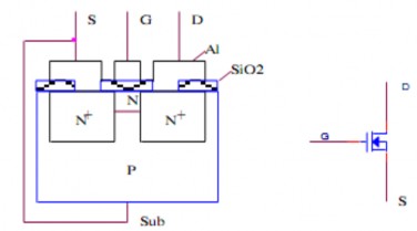
Figure 3-50. Structure – symbol of N-type continuous channel MOSFET.
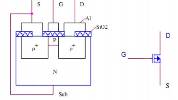
Figure 3-51. Structure - symbol of P-type continuous channel MOSFET. Gate (G): gate pole (gate pole)
Drain (D): drain pole (drain pole) Source (S): source pole Substrate (Sub): base (base)
N-type continuous channel MOSFET structure
On the P-type semiconductor substrate, two high-concentration N-type semiconductor regions (N+) are mixed, connected by a low-concentration N-type semiconductor region (N). A thin layer of SiO2, an insulator, is coated on top.
The two N+ semiconductor regions in contact with the metal (Al) give rise to the drain (D) and source (S) terminals. The G terminal has metal contact outside the oxide layer but is still insulated from the N channel which means the impedance to the terminal is large.
To distinguish between N or P channels, the manufacturer adds a fourth pin called the Sub pin, which joins the channel to form a PN junction. In fact, the Sub pin of the MOSFET is connected by the manufacturer to the S pole inside the MOSFET.
b. Characteristics
V DS is the voltage between the D and S poles. V GSis the voltage between the G and S poles. Consider the circuit as (Figure 3-52)
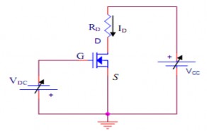
Figure 3-52. Circuit to investigate the characteristics of a continuous-channel N-type MOSFET.
When V GS = 0V: electrons move to create current I D , when increasing voltage V DS , current I D increases, I D will increase to a limit value I Dsa t (current I D saturation). Voltage V DS at value I Dsat is called choke voltage V P0 like JFET.
When V GS < 0: the G pole has a negative potential, so it pushes electrons in the N channel into the P region, narrowing the cross-section of the N conduction channel and the I D current will decrease due to increased channel resistance.
As the gate voltage becomes more negative, the I D current becomes smaller, and at a certain limit value the I D current almost disappears. This voltage at the gate is called the blocking voltage –V P0 . This transfer characteristic is similar to the transfer characteristic of an N-channel JFET.
When V GS > 0, the G pole has a positive potential, the minority electrons in the P base region are attracted to the N channel, increasing the channel cross-section, the channel resistance is reduced and the I D current
increase higher than saturation value I Dsat . In this case, large I D can easily damage MOSFET so it is rarely used.
Similar to JFET, we examine two types of characteristics of continuous channel MOSFET:
- Transmission characteristic I D (V GS ) corresponding to V DS = const.
- Output characteristic I D (V DS ) corresponding to V GS = const.
The survey method is similar to JFET survey but when V GS is needed> 0, we change the polarity of the V DC source , but note that if the positive source is small, then I Dhas increased. We have two types of characteristics.
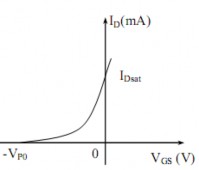
Figure 3-53. Transmission characteristic I D (V GS ) of a continuous-channel N-type MOSFET.
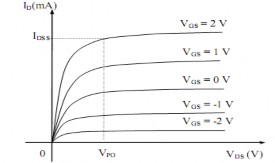
Figure 3-54. Output characteristic I(V) of N-type continuous-channel MOSFET.
5.2.2. Discontinuous channel MOSFET
a. Structure - symbols:
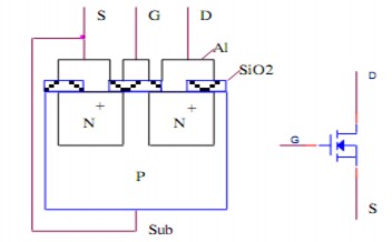
Figure 3-55. Structure - symbol of N-type interrupted channel MOSFET.
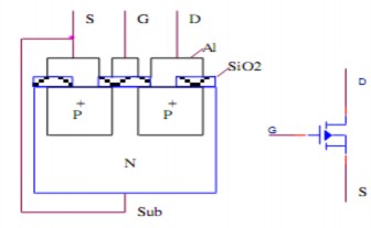
Figure 3-56. Structure - symbol of P-type interrupted channel MOSFET.
Gate (G); Drain (D); Source (S); Substrate (Sub)
The structure of the N-type interrupted channel MOSFET is similar to the structure of the N-type continuous channel MOSFET but does not have an N channel. This means that the two high-concentration (N+) N-type semiconductor regions are not connected to each other, so it is also called interrupted channel MOSFET. The top surface of the conductive channel is also covered with a layer of SiO2 insulating oxide. The two conductors that pass through the insulating layer and connect to the N+ semiconductor region are called the S and D poles. The G pole is taken from the metal that is in contact with the outside of the SiO2 oxide layer but is insulated from the inside. The Sub pole is connected to the S pole inside the MOSFET.
b. Characteristics
Consider the following circuit: .
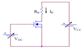
Figure 3-57. Circuit to investigate the characteristics of an N-type discontinuous channel MOSFET.
When V GS = 0V, electrons cannot move so I D = 0, the resistance between D and S is very large. When V GS > 0V, the positive charge at the G pole will attract electrons from the P base towards the middle of the two N+ semiconductor regions and when the attraction is large enough, the number of electrons attracted is greater, enough to connect the two N+ semiconductor regions and the N channel connecting the two N+ semiconductor regions is formed, so there is a current I D running from D to S. The higher the G pole voltage is, the larger I D becomes.
The threshold potential V is the potential V GS large enough to form a channel, usually
V several volts.
Similar to JFET and continuous channel MOSFET, we examine two types of characteristics of discrete channel MOSFET:
- Transmission characteristic I D (V GS ) corresponding to V DS = const.
- Output characteristic I D (V DS ) corresponding to V GS = const.
The investigation method is similar to the investigation of JFET and continuous channel MOSFET, but different from the two cases above, it requires V GS > 0, specifically the DC source V must be positive enough for V GS to equal the threshold voltage V , then ID has a value other than 0. We have two types of characteristics as (Figure 3-58) and (Figure 3-59)
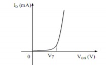
Figure 3-58. Transmission characteristic I D (V GS ) of an N-type discontinuous channel MOSFET.
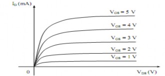
Figure 3-59. Output characteristic I(V) of N-type discontinuous channel MOSFET.
5.2.3. Basic connections of MOSFET
Similar to JFET, MOSFET also has three basic connection types:
- Common source pole CS: Input signal G vs S, output signal D vs S.
- Common gate CG: Input signal S vs G, output signal D vs G.
- Common drain CD: Input signal G vs D, output signal S vs D.
5.3 Application
As presented above, FET has two types: JFET and MOSFET, both of which operate based on controlling the conductivity of the semiconductor sample by an external electric field, using only one type of conductor (majority carrier), it is unipolar, there is no generation and recombination process of two types of conductors, so the parameters of FET are less affected by temperature.
Outstanding advantages of FET: large input impedance, high amplification factor, low energy consumption, the size of D, G, S electrodes can be reduced to very small, significantly reducing the volume of FET and it is widely used in IC manufacturing, especially ICs with high integration density. Like BJT, FET is widely used in both digital and analog circuits. It is an element in many types of amplifier circuits, electronic switches, etc.
In addition, the FET family also has the following forms: CMOS, V-MOS, D-MOS, FET,... these are improved forms of MOSFET to have more advantages in application.
Overview of Transistors
Transistor Type
Operation Type Symbol
BIPOLAR
JFET
POOR TYPE MOSFET
c
e
bNPN

c
b PNP
e
S
D
G NJFET
D
S
G PJFET
S
D
G2N3796
D
G PMOS
S
Normally the transistor does not conduct but a small current flows in and a small positive voltage at the base makes the emitter conduct (allowing a large amount of current to flow from the collector to the emitter). The transistor operates under the condition V C > V E. Used in switching and amplification applications.
Usually the transistor does not conduct, but with a current
small output and small negative voltage at the base makes the emitter conduct (allowing a large amount of current to flow from the emitter to the collector). The transistor operates with V E > V C . Used as switching and amplification.
Normally the transistor conducts, but with a negative voltage
small at the gate G causes the source S to stop conducting (not allowing current from the source S to flow to the drain D). The transistor operates under the condition that V D > V S. No gate current is required. Used as a switch and amplifier.
Usually the transistor conducts, but with a voltage
small positive voltage at the gate G causes the source to stop conducting (not allowing current from the source S to flow to the drain D). The transistor operates under the condition that V S > V D . No gate current is required
G. Used as a switch and amplifier. Usually the MOSFET transistor is a poor conductor, but with a small negative voltage applied to the gate G, the source gate S stops conducting (stopping the large current flowing through the drain D - source S). The transistor operates under the condition that V D > V S. No gate current is required. Used in switching and amplifier applications.
Usually MOSFET transistors are of the depletion type, but
with a small positive voltage applied to the gate G, causing the source gate S to stop conducting (stopping the large current flowing through the source S - drain D). The transistor operates under the condition that V S > V D. No gate current is required. Used as a switch
circuit and amplifier.
RICH TYPE MOSFET
D
G2N3796
S
D
GIRF9510
S
B2
Usually, the MOSFET transistor is rich in conduction, but with a small positive voltage applied to the gate G, the source gate S conducts (allowing a large current to flow through the drain D - source S). The transistor operates under the condition that V D > V S. No gate current is required. Used as a switch and amplifier.
Usually the MOSFET transistor is rich in conduction,
but with a small negative voltage applied to the gate G, the source gate S conducts (allowing a large current to flow through the source S - drain D). The transistor operates under the condition that V S > V D. No gate current is required. Used as a switch and amplifier.
There is usually a very small current flowing from the base terminal B 2 to
UJT E
UJT
base terminal B 1 , but a positive voltage applied to the emitter terminal E causes base terminal B 1 or base terminal B 2
B1increase the flow. The transistor operates under the condition V B2 > V B1 . No gate current is required.
Acts as a switch only.
6. SCR – Triac- Diac
Target:
- Present the structure, operating principle, characteristics of Thyristor, TRIAC, DIAC
- Draw diagrams of Thyristor, TRIAC, DIAC connections and present the operating principles of the circuit.
6.1. Thyristor (Silicon Controlled Rectifier = SCR)
a. Structure - symbols
SCR (Silicon Controlled Rectifier) is composed of four layers of semiconductor P, N joined alternately to create three P - N junctions or three contact layers J1, J2, J3 and connected to three legs. (Figure 3-60)
A: Anode: positive pole K: Cathode: negative pole
G: Gate: control terminal (gate terminal)