The resistance of the two transitions J E and J C is very small, the current through the Transistor is current I.C
large and close to the saturation current.
very
The gain mode is to use the transistor as a linear element to amplify the signal, while the saturation mode and the clipping mode the transistor acts as an electronic switch with two on and off states.
Transistor stops conducting
Maybe you are interested!
-

 Basic Electronic Engineering - Ho Chi Minh City College of Construction Part 2 - 7
 -
 Basic Electronic Engineering - Ho Chi Minh City College of Construction Part 1 - 11
 -
 Electronic Engineering - Ho Chi Minh City College of Transport - 31
 -
 Basic electronic engineering - City College of Construction. HCM Part 1 - 1
 -
 Basic factors affecting household education spending in Ho Chi Minh City - 9
V + Poor Area
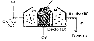
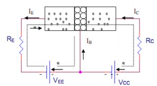
Figure 3-30. Description of the transistor's cut-off state
Figure 3-31. Description of the conduction state of the transistor From the above description, we have the following current relationship in the transistor:
-I.E. I B I C
- Current amplification factor in DC mode:
I C .
I
DC
B
is usually a constant value of 10 500 but can vary with temperature and with collector – emitter voltage.
- Current transfer coefficient in DC mode: I C
I
DC
E
=> DC
DC
DC 1
=> DC
DC
1
DC
4.2 Basic properties
4.2.1. Important rules:
Rule 1: For an npn transistor, the voltage at the collector V C must be greater than the voltage at the emitter VE by at least a few tenths of a volt, otherwise no current will flow across the collector-emitter junction. For a pnp transistor, the emitter voltage must be greater than the collector voltage by the same amount.
Rule 2: For an npn transistor, there is a 0.6 V base-to-emitter voltage drop. For a pnp transistor, there is a 0.6 -V voltage rise from base to emitter. In operational terms, this means that the base voltage V B of an npn transistor must be at least 0.6 V greater than the V E voltage ; otherwise the transistor will not pass a current through the emitter-collector. For a pnp transistor, V B must be at least 0.6 V less than the V E voltage ; otherwise the transistor will not pass a current from the collector to the emitter.
4.2.2. Basic ways of connecting transistors
In electrical circuits, the BJT is considered as a 4-terminal network: the signal is input on two terminals and the signal is also taken out on two terminals.
BJT has 3 terminals: E, B, C, so when using, we must place one terminal as the common wire of the input and output circuits. We can choose one of the 3 terminals to be the common terminal for the input and output circuits. Therefore, Transistors have 3 basic connections: common emitter (CE), common base (CB), and common collector (CC).
Common Emitter Circuit (Common Emitter ≡ CE) (Figure 3-32)
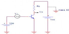
Figure 3-32. BJT connected in common emitter mode.
BJT is connected in common base mode (Common Base ≡ CB) . (Figure 3-33)
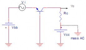
Figure 3-33. BJT connected in common base mode.
BJT connected in common collector mode (Common Collector ≡ CC) . (Figure 3-34)
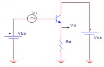
Figure 3-34. BJT connected in common collector mode.
CE: -Input signal B vs E, output signal C vs E
- Phase between input and output signals: phase inversion.
- Large Ai, Av amplification factor.
CB: -Input signal E compared to B, output signal C compared to B
- Phase between input and output signals: in phase.
- Large amplification factor Av, Ai ≈ 1.
CC: - Input signal B compared to C, output signal E compared to
- Phase between input and output signals: in phase.
- Large amplification factor Ai, Av ≈ 1.
4.2.3. BJT characteristics (figure 3-35)
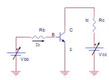
Figure 3-35. Circuit to examine the characteristics of BJT.
Consider the circuit as shown in Figure 3.25. With V BE being the voltage between the base terminal B and the emitter terminal
E. V CE is the voltage between collector C and emitter E.
Input characteristic I B (V BE ) corresponding to V CE = const
Select a positive source V CC to have V CE = const. Adjust the source V BB to change V BE from 0 to a value less than the threshold voltage Vγ, then measure the current I B.
≈ 0. Continue to increase the source V BB to have V BE = Vγ, then the current I B starts to appear and I B also increases exponentially like the current I D of the forward biased diode. (Figure 3-36)
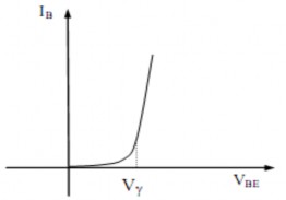
Figure 3-36. Input characteristics of BJT
Transmission characteristic IC ( V BE ) corresponding to V CE = const
To investigate this characteristic, we measure and adjust the source to be similar to the input characteristic but measure the current I C , and observe how I C changes when V BE changes. We have a transmission characteristic I C (V BE ) that has the same form as the input characteristic I B ( V BE ) but the current I C has a value many times larger than I B.
I C = I B
Output characteristic IC ( V CE ) corresponding to I B = const
The source V BB forward biases the P – N junction between B and E to create current I B . When the voltage V B < V ie V BE < V then the current I B = 0 and I C = 0 even though the source is increased. When
voltage V BE ≥ V then the current I B ≠ 0. Change V BB so that I B has a certain value, use a meter, suppose to measure I B = 15 A. At this time keep I B fixedby keeping V BB constant , then changing V CC → V CE changes, measure the I C current corresponding to the V CE change.
Initially, I C increases rapidly with V CE , but at a value of about I C = I B , I C almost does not increase even though the voltage V CE increases a lot.
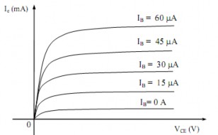
Figure 3-37. BJT output characteristics
If we want I C to increase higher, we must increase V BB to get a higher increase in I B. We continue to change V CC to measure I C accordingly. We also see that at first I C increases rapidly according to V CE , but at the saturation value I C = I B , I C almost does not increase even though V CE still increases.
Similar survey of I C (V CE ) at different I B values , we have the output characteristics as (Figure 3-27)
Above we have considered the characteristics of BJT connected in CE type. We can also consider the characteristics of BJT connected in other types:
BJT connected in CB type:
- Input characteristic IE ( V EB ) corresponding to V CB = const.
- Transmission characteristic IC ( V EB ) corresponding to V CB = const.
- Output characteristic IC ( V CB ) corresponds to IE = const.
BJT connected in CC mode:
- Input characteristic I B (V BC ) corresponding to V EC = const.
- Transmission characteristic IE ( V BC ) corresponding to V EC = const.
- Output characteristic IE ( V EC ) corresponding to I B = const.
4.2.4 BJT bias
BJT has many applications in electronic devices, depending on each specific application, BJT needs to provide voltage and current to each leg appropriately.
Biasing is applying voltage to the BJT terminals. BJT biasing is choosing the DC power source and resistor so that I B , I C , V CE have appropriate values as required.
Conditions for BJT to conduct electricity:
- The P – N junction between B and E (junction J E ) is forward biased.
- The P – N junction between B and C (J C junction ) is reverse biased.
- VBE threshold voltage depends on BJT type.
NPN type BJT:
V BE = 0.6 V (0.7 V) (Si) ,V BE = 0.2 V (0.3 V) (Ge) V CE � ( ⅓V CC ÷ ⅔V CC ) .
PNP type BJT:
V EB = 0.6 V (0.7 V) (Si) ,V EB = 0.2 V (0.3 V) (Ge) V EC � ( ⅓V CC ÷ ⅔V CC )
4.2.4.1. Use two separate sources
The source V BB is forward biased at the BE junction. The source V CC is combined with V BB to reverse bias the BC junction. The above circuit has been designed, now we calculate I B , I C , V CE to determine the operating point in the static state of the BJT according to the design. (Figure 3-38)
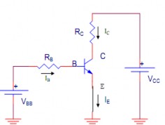
Figure 3-38. BJT bias circuit using two sources with emitter connected to ground.
Considering the Base-emiter circuit, we have: V
I . R U
=> I
V BB U BE
(3.1)
BB BB BE
B
I C I B
Consider the Collector circuit: V CC I C . R C V CE
B
R
(3.2)
= > V C E V C C I C.R C
. Static load line equation . (3.3)
Note: R C , V CC = const so when V CE increases, I C decreases and vice versa. To draw the static load curve, we determine 2 points:
First point: I C = 0 =>
V CE
V CC
Second point: V CE
= 0 =>
I C
V CC R
C
When BJT amplifies small amplitude signals, it is appropriate to bias the Q point so that it is about halfway between the static load line.
Determine the voltage at the terminals of the BJT: V E = 0V
V B
V E V B E
0.6V
(3.4)
VC VC – IC R C
In case of additional resistor R E : .(figure 3-39)
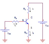
Figure 3-39. BJT bias circuit using two sources with R E . Considering the Base-emitter loop, we have: V B B I B. R BU B E I.E.. R E
=I B. R B U B E ( I B I C). R E=I B. R B U B E I B(1 ). R E
=I B. R B U B E I B. . R E
(3.5)
Because >> so 1+ .=>
I V BB U BE
B
R B
=> I
C . I B
Consider the Collector circuit: V C C I C. R C V C E I.E.. R E
=I B. R B U B E IC. R E
= > V C E V C C I C(R C R E)
I
V BB V BE
BR
. R
�
Coordinates of the polarization point Q : Q
BEIGE
I C . I B
(3.6)
V V I ( R R )
CE CC CCE
�
Static load line equation: V C E V C C I C( R BR E)
(3.7)
Comment: R C , R E , V CC = const so when V CE increases, I C decreases and vice versa. Draw the static load curve:
I C = 0 => V CE = V CC
V CE
= 0 =>
I C
V CC R C R E
The static load line is a straight line passing through two points: A(Vcc,0) , B( Voltage at the terminals of the BJT:
V CC R C R E
,0).
V E I E .R E
V V V
BE BE
(3.18)
V
�
CV CC
– I C .R C
4.2.4.2. Use a single source
a. Use voltage reducing resistor R B .(Figure 3-40)
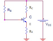
Figure 3-40. BJT bias circuit using voltage drop resistor RB .
We have: V C C I B. R B U B E IE.R E=I B. R B U B E (I B+I C).R E
I . R U I . .R
=> I
V BB V BE
BB BE B E
BR . R
BEIGE
=> I C . I B
V C C V C E I C( R C R E) = > V C E V C C I C( R C R E)
I
V BB V BE
BR
. R
�
Coordinates of the polarization point: Q
BEIGE
I C . I B
(3.19)
V V I ( R R )
CE CC CCE
�
Static load line equation: V C E V C C I C( R CR E). (3.20) Comment: R C ,V C C = const so if V C E increases then I Cdecrease and vice versa.
Draw static load curve graph:
I C = 0 => V CE = V CC
V CE
= 0 =>
I C
V CC R C R E