air to increase the contact ability and stability between Ag 2 O nanoparticles and SnO 2 nanowires .
Ag 2 O oxide is a p- type semiconductor oxide . Therefore, in the fabricated sensor, a heterojunction layer of different n-p carrier type is formed at the contact surface between the two oxides, Ag 2 O and SnO 2 .
2.2.3. Fabrication of heterostructured SnO 2 /ZnO nanowires
Maybe you are interested!
-
 Car body electrical practice - 8
zt2i3t4l5ee
zt2a3gs
zt2a3ge
zc2o3n4t5e6n7ts
If the voltage is out of specification, replace the wire or connector.
If the voltage is within specification, install the front fog light relay and follow step 5.
Step 5 Check the front fog light switch
- Remove the D4 connector of the fog light switch
- Use a multimeter to measure the resistance of the front fog light switch.
Measurement location
Condition
Standard
D4-3 (BFG) -D4-4 (LFG)
Light switchFront Fog OFF
>10kΩ
D4-3 (BFG) -D4-4 (LFG)
Front fog light switchON
<1 Ω
- Standard resistor
D4 connector is located on the combination switch assembly.
If the resistance is out of specification, replace the combination switch (the fog light switch is located in the combination switch).
If the resistance is within specification, follow step 6.
Step 6 Check wiring and connectors (front fog light relay-light selector switch)
- Disconnect connector D4 of the combination switch assembly
- Use a voltmeter to measure the voltage value of jack D4 on the wire side.
Measurement location
Control modecontrol
Standard
D4-3 (BFG) - (-) AQ
TAIL
11 to 14 V
D4 connector for the wiring of the combination switch assembly
If the voltage does not meet the standard, replace the wire or connector.
If the voltage is within standard, there may have been an error in the previous measurements.
Step 7 Check the front fog lights
- Remove the front fog light electrical connector.
- Supply battery voltage to the fog lamp terminals
Jack 8, B9 of front fog lamp on the electrical side
blind first.
Power supply location
Terms and Conditions
Battery positive terminal - Terminal 2Battery negative terminal - Terminal 1
Fog lightsbefore morning
- If the light does not come on, replace the bulb.
If the light is on, re-plug the jack and continue to step 8.
Step 8 Check wiring and connectors (relay and front fog lights)
- Disconnect the B8 and B9 connectors of the front fog lights.
- Use a voltmeter to measure voltage at the following locations:
Measurement location
Switch location
Terms and Conditions
B8-2 - (-) AQ
Electric lock ON TAIL size switchFog switch ON
11 to 14 V
B9-2 - (-) AQ
Electric lock ONTAIL size switch Fog switch ON
11 to 14 V
B8 and B9 connectors on the front fog lamp wiring side
Voltage is not up to standard, repair or replace the jack. If up to standard, there may have been an error in the measurement process.
2.2.4. Procedure for removing, installing and adjusting fog lights 1. Procedure for removing
- Remove the front inner ear pads
Use a screwdriver to remove the 3 screws and remove the front part of the front inner ear liner
-Remove the fog light assembly
+ Disconnect the connector.
+ Use a screwdriver to remove 3 screws to remove the fog light cover
2. Installation sequence
-Rotate the fog lamp bulb in the direction indicated by the arrow as shown in the figure and remove the fog lamp from the fog lamp assembly.
-Rotate the fog light bulb in the direction indicated by the arrow as shown in the figure and install the light into the fog light assembly.
- Use a screwdriver to install the fog light cover
-Install the electrical connector
Attention: Be careful not to damage the plastic thread on the lamp assembly.
- Install the front inner ear pads
Use a screwdriver to install the front inner bumper with 3 screws.
3. Prepare the vehicle to adjust the fog light convergence. Prepare the vehicle:
- Make sure there is no damage or deformation to the vehicle body around the fog lights.
- Add fuel to the fuel tank
- Add oil to standard level.
- Add engine coolant to standard level.
- Inflate the tire to standard pressure.
- Place spare tire, tools and jack in original design position
- Do not leave any load in the luggage compartment.
- Let a person weighing about 75 kg sit in the driver's seat.
4. Prepare to check the fog light convergence
a/ Prepare the vehicle status as follows:
- Place the car in a dark enough place to see the lines. The lines are the dividing line, below which the light from the fog lights can be seen but above which it cannot.
- Place the car perpendicular to the wall.
- Keep a distance of 7.62 m between the center of the fog lamp and the wall.
- Park the car on level ground.
- Press the car down a few times to stabilize the suspension.
Note: A distance of approximately 7.62 m is required between the vehicle (fog lamp center) and the wall to adjust the convergence correctly. If the distance of 7.62 m cannot be achieved, set the correct distance of 3 m to check and adjust the fog lamp convergence. (Since the target area varies with the distance, please follow the instructions as shown in the figure.)
b/ Prepare a piece of thick white paper about 2 m high and 4 m wide to use as a screen.
c/ Draw a vertical line through the center of the screen (line V).
d/ Set the screen as shown in the picture. Note:
- Keep the screen perpendicular to the ground.
- Align the V line on the screen with the center of the vehicle.
e/Draw the reference lines (H, V LH and V RH lines) on the screen as shown in the figure.HINT:
Mark the center of the fog lamp on the screen. If the center mark cannot be seen on the fog lamp, use the center of the fog lamp or the manufacturer's name mark on the fog lamp as the center mark.
H line (fog light height):
Draw a line across the screen so that it passes through the center mark. Line H should be at the same height as the center mark of the fog light bulb.
Line V LH, V RH (center mark position of left fog lamp LH and right fog lamp RH):
Draw two lines so that they intersect line H at the center marks.
5. Check the fog light convergence
a/ Cover the fog lamp or remove the connector of the other side fog lamp to prevent light from the unchecked fog lamp from affecting the fog lamp convergence test.
b/ Start the engine.
c/ Turn on the fog lights and make sure that the dividing line is outside the standard area as shown in the drawing.
6. Adjust the fog light convergence
Use a screwdriver to adjust the fog light to the standard area by turning the toe adjustment screw.
Note: If the screw is adjusted too far, loosen it and then tighten it again, so that the last rotation of the light adjustment screw is clockwise.
3. Self-study questions
1. Describe the operating principle of the lighting system with automatic headlight function
2. Describe the operating principle of the lighting system with the function of rotating headlights when turning
3. Draw diagram and connect lighting system on Hyundai Porter car
4. Draw diagram and connect lighting system on Honda Accord 1992
5. Draw the lighting circuit on a 1993 Toyota Lexus
LESSON 3 MAINTENANCE AND REPAIR OF SIGNAL SYSTEM
I. IMPLEMENTATION GOAL
After completing this lesson, students will be able to:
- Distinguish between types of signals on cars
- Correctly describe common symptoms and suspected areas causing damage.
- Connecting signal circuits ensures technical requirements
- Disassemble, install, check, maintain and repair the signal system to ensure technical requirements.
- Ensure safety in work and industrial hygiene
II. LESSON CONTENT
1. General description
The signal system equipped on cars aims to create signals to notify other vehicles participating in traffic about the vehicle's operating status such as: stopping, parking, braking, reversing, turning...
Signals are used either by light such as headlamps, brake lights, turn signals….. or by sound such as horns, reverse music….
Just like the lighting system. A signal system circuit usually consists of: battery, fuse, wire, relay, electrical load and control switch. Only some switches of the signal system are on the combination switch. The switches of other signals are usually located in different locations such as in the gearbox or brake pedal……
2. Maintenance and repair
2.1. Turn signals and hazard lights
The installation location of the turn signal is shown in Figure 3.1. The turn signal control switch is located in the combination switch under the steering wheel. Turning this switch to the right or left will make the turn signal turn right or left.
The hazard light switch is used when the vehicle has a problem while participating in traffic. When the hazard light switch is turned on, all the turn signals on the vehicle will light up at a certain frequency. The hazard light switch is usually placed separately from the turn signal switch (some old cars integrate the hazard and turn signal switches on the same combination switch cluster).
Figure 3.1 Turn signal switch Figure 3.2 Hazard switch
The part that generates the flashing frequency for the lights is called a turn signal relay. The turn signal relay usually has 3 terminals: B (positive power supply); E (negative power supply); L (providing the turn signal switch to distribute to the
lamp)
2.1.1. Circuit diagram
To generate the frequency for the turn signal, a turn signal relay is used in the turn signal circuit. The current from the turn signal relay will be sent to the turn signal switch assembly to distribute the current to the turn signal lights for the driver's purpose.
Figure 3.3. Schematic diagram of a turn signal circuit without a hazard switch
1. Battery; 2. Electric lock; 3. Turn signal relay; 4. Turn signal switch; 5. Turn signal lamp; 6. Turn signal lamp; 7. Hazard switch
Figure 3.4 Schematic diagram of turn signal circuit with hazard switch
1. Battery; 2. Combination switch cluster; 3. Turn signal;
4. Turn signal light; 5. Turn signal relay
Today's cars no longer use three-pin turn signal relays (B, L, E) but use eight-pin turn signal relays (figure 3.5) (pin number 8 is used for hazard lights).
For this type, the current supplying the turn signal lights is supplied directly from the turn signal relay to the lights.
div.maincontent .p { color: black; font-family:"Times New Roman", serif; font-style: normal; font-weight: normal; text-decoration: none; font-size: 14pt; margin:0pt; } div.maincontent p { color: black; font-family:"Times New Roman", serif; font-style: normal; font-weight: normal; text-decoration: none; font-size: 14pt; margin:0pt; } div.maincontent .s1 { color: black; font-family:"Times New Roman", serif; font-style: normal; font-weight: normal; text-decoration: none; font-size: 13pt; } div.maincontent .s2 { color: black; font-family:"Times New Roman", serif; font-style: italic; font-weight: normal; text-decoration: none; font-size: 14pt; } div.maincontent .s3 { color: black; font-family:"Times New Roman", serif; font-style: normal; font-weight: normal; text-decoration: none; font-size: 14pt; } div.maincontent .s4 { color: black; font-family:"Times New Roman", serif; font-style: normal; font-weight: normal; text-decoration: none; font-size: 13pt; } div.maincontent .s5 { color: black; font-family:"Times New Roman", serif; font-style: normal; font-weight: normal; text-decoration: none; font-size: 13pt; vertical-align: 1pt; } div.maincontent .s6 { color: black; font-family:"Times New Roman", serif; font-style: normal; font-weight: normal; text-decoration: none; font-size: 11pt; } div.maincontent .s7 { color: black; font-family:"Times New Roman", serif; font-style: normal; font-weight: normal; text-decoration: none; font-size: 14pt; vertical-align: -9pt; } div.maincontent .s8 { color: black; font-family:"Times New Roman", serif; font-style: normal; font-weight: normal; text-decoration: none; font-size: 11pt; } div.maincontent .s9 { color: #008000; font-family:"Times New Roman", serif; font-style: normal; font-weight: normal; text-decoration: none; font-size: 14pt; } div.maincontent .s10 { color: black; font-family:"Times New Roman", serif; font-style: italic; font-weight: normal; te
Car body electrical practice - 8
zt2i3t4l5ee
zt2a3gs
zt2a3ge
zc2o3n4t5e6n7ts
If the voltage is out of specification, replace the wire or connector.
If the voltage is within specification, install the front fog light relay and follow step 5.
Step 5 Check the front fog light switch
- Remove the D4 connector of the fog light switch
- Use a multimeter to measure the resistance of the front fog light switch.
Measurement location
Condition
Standard
D4-3 (BFG) -D4-4 (LFG)
Light switchFront Fog OFF
>10kΩ
D4-3 (BFG) -D4-4 (LFG)
Front fog light switchON
<1 Ω
- Standard resistor
D4 connector is located on the combination switch assembly.
If the resistance is out of specification, replace the combination switch (the fog light switch is located in the combination switch).
If the resistance is within specification, follow step 6.
Step 6 Check wiring and connectors (front fog light relay-light selector switch)
- Disconnect connector D4 of the combination switch assembly
- Use a voltmeter to measure the voltage value of jack D4 on the wire side.
Measurement location
Control modecontrol
Standard
D4-3 (BFG) - (-) AQ
TAIL
11 to 14 V
D4 connector for the wiring of the combination switch assembly
If the voltage does not meet the standard, replace the wire or connector.
If the voltage is within standard, there may have been an error in the previous measurements.
Step 7 Check the front fog lights
- Remove the front fog light electrical connector.
- Supply battery voltage to the fog lamp terminals
Jack 8, B9 of front fog lamp on the electrical side
blind first.
Power supply location
Terms and Conditions
Battery positive terminal - Terminal 2Battery negative terminal - Terminal 1
Fog lightsbefore morning
- If the light does not come on, replace the bulb.
If the light is on, re-plug the jack and continue to step 8.
Step 8 Check wiring and connectors (relay and front fog lights)
- Disconnect the B8 and B9 connectors of the front fog lights.
- Use a voltmeter to measure voltage at the following locations:
Measurement location
Switch location
Terms and Conditions
B8-2 - (-) AQ
Electric lock ON TAIL size switchFog switch ON
11 to 14 V
B9-2 - (-) AQ
Electric lock ONTAIL size switch Fog switch ON
11 to 14 V
B8 and B9 connectors on the front fog lamp wiring side
Voltage is not up to standard, repair or replace the jack. If up to standard, there may have been an error in the measurement process.
2.2.4. Procedure for removing, installing and adjusting fog lights 1. Procedure for removing
- Remove the front inner ear pads
Use a screwdriver to remove the 3 screws and remove the front part of the front inner ear liner
-Remove the fog light assembly
+ Disconnect the connector.
+ Use a screwdriver to remove 3 screws to remove the fog light cover
2. Installation sequence
-Rotate the fog lamp bulb in the direction indicated by the arrow as shown in the figure and remove the fog lamp from the fog lamp assembly.
-Rotate the fog light bulb in the direction indicated by the arrow as shown in the figure and install the light into the fog light assembly.
- Use a screwdriver to install the fog light cover
-Install the electrical connector
Attention: Be careful not to damage the plastic thread on the lamp assembly.
- Install the front inner ear pads
Use a screwdriver to install the front inner bumper with 3 screws.
3. Prepare the vehicle to adjust the fog light convergence. Prepare the vehicle:
- Make sure there is no damage or deformation to the vehicle body around the fog lights.
- Add fuel to the fuel tank
- Add oil to standard level.
- Add engine coolant to standard level.
- Inflate the tire to standard pressure.
- Place spare tire, tools and jack in original design position
- Do not leave any load in the luggage compartment.
- Let a person weighing about 75 kg sit in the driver's seat.
4. Prepare to check the fog light convergence
a/ Prepare the vehicle status as follows:
- Place the car in a dark enough place to see the lines. The lines are the dividing line, below which the light from the fog lights can be seen but above which it cannot.
- Place the car perpendicular to the wall.
- Keep a distance of 7.62 m between the center of the fog lamp and the wall.
- Park the car on level ground.
- Press the car down a few times to stabilize the suspension.
Note: A distance of approximately 7.62 m is required between the vehicle (fog lamp center) and the wall to adjust the convergence correctly. If the distance of 7.62 m cannot be achieved, set the correct distance of 3 m to check and adjust the fog lamp convergence. (Since the target area varies with the distance, please follow the instructions as shown in the figure.)
b/ Prepare a piece of thick white paper about 2 m high and 4 m wide to use as a screen.
c/ Draw a vertical line through the center of the screen (line V).
d/ Set the screen as shown in the picture. Note:
- Keep the screen perpendicular to the ground.
- Align the V line on the screen with the center of the vehicle.
e/Draw the reference lines (H, V LH and V RH lines) on the screen as shown in the figure.HINT:
Mark the center of the fog lamp on the screen. If the center mark cannot be seen on the fog lamp, use the center of the fog lamp or the manufacturer's name mark on the fog lamp as the center mark.
H line (fog light height):
Draw a line across the screen so that it passes through the center mark. Line H should be at the same height as the center mark of the fog light bulb.
Line V LH, V RH (center mark position of left fog lamp LH and right fog lamp RH):
Draw two lines so that they intersect line H at the center marks.
5. Check the fog light convergence
a/ Cover the fog lamp or remove the connector of the other side fog lamp to prevent light from the unchecked fog lamp from affecting the fog lamp convergence test.
b/ Start the engine.
c/ Turn on the fog lights and make sure that the dividing line is outside the standard area as shown in the drawing.
6. Adjust the fog light convergence
Use a screwdriver to adjust the fog light to the standard area by turning the toe adjustment screw.
Note: If the screw is adjusted too far, loosen it and then tighten it again, so that the last rotation of the light adjustment screw is clockwise.
3. Self-study questions
1. Describe the operating principle of the lighting system with automatic headlight function
2. Describe the operating principle of the lighting system with the function of rotating headlights when turning
3. Draw diagram and connect lighting system on Hyundai Porter car
4. Draw diagram and connect lighting system on Honda Accord 1992
5. Draw the lighting circuit on a 1993 Toyota Lexus
LESSON 3 MAINTENANCE AND REPAIR OF SIGNAL SYSTEM
I. IMPLEMENTATION GOAL
After completing this lesson, students will be able to:
- Distinguish between types of signals on cars
- Correctly describe common symptoms and suspected areas causing damage.
- Connecting signal circuits ensures technical requirements
- Disassemble, install, check, maintain and repair the signal system to ensure technical requirements.
- Ensure safety in work and industrial hygiene
II. LESSON CONTENT
1. General description
The signal system equipped on cars aims to create signals to notify other vehicles participating in traffic about the vehicle's operating status such as: stopping, parking, braking, reversing, turning...
Signals are used either by light such as headlamps, brake lights, turn signals….. or by sound such as horns, reverse music….
Just like the lighting system. A signal system circuit usually consists of: battery, fuse, wire, relay, electrical load and control switch. Only some switches of the signal system are on the combination switch. The switches of other signals are usually located in different locations such as in the gearbox or brake pedal……
2. Maintenance and repair
2.1. Turn signals and hazard lights
The installation location of the turn signal is shown in Figure 3.1. The turn signal control switch is located in the combination switch under the steering wheel. Turning this switch to the right or left will make the turn signal turn right or left.
The hazard light switch is used when the vehicle has a problem while participating in traffic. When the hazard light switch is turned on, all the turn signals on the vehicle will light up at a certain frequency. The hazard light switch is usually placed separately from the turn signal switch (some old cars integrate the hazard and turn signal switches on the same combination switch cluster).
Figure 3.1 Turn signal switch Figure 3.2 Hazard switch
The part that generates the flashing frequency for the lights is called a turn signal relay. The turn signal relay usually has 3 terminals: B (positive power supply); E (negative power supply); L (providing the turn signal switch to distribute to the
lamp)
2.1.1. Circuit diagram
To generate the frequency for the turn signal, a turn signal relay is used in the turn signal circuit. The current from the turn signal relay will be sent to the turn signal switch assembly to distribute the current to the turn signal lights for the driver's purpose.
Figure 3.3. Schematic diagram of a turn signal circuit without a hazard switch
1. Battery; 2. Electric lock; 3. Turn signal relay; 4. Turn signal switch; 5. Turn signal lamp; 6. Turn signal lamp; 7. Hazard switch
Figure 3.4 Schematic diagram of turn signal circuit with hazard switch
1. Battery; 2. Combination switch cluster; 3. Turn signal;
4. Turn signal light; 5. Turn signal relay
Today's cars no longer use three-pin turn signal relays (B, L, E) but use eight-pin turn signal relays (figure 3.5) (pin number 8 is used for hazard lights).
For this type, the current supplying the turn signal lights is supplied directly from the turn signal relay to the lights.
div.maincontent .p { color: black; font-family:"Times New Roman", serif; font-style: normal; font-weight: normal; text-decoration: none; font-size: 14pt; margin:0pt; } div.maincontent p { color: black; font-family:"Times New Roman", serif; font-style: normal; font-weight: normal; text-decoration: none; font-size: 14pt; margin:0pt; } div.maincontent .s1 { color: black; font-family:"Times New Roman", serif; font-style: normal; font-weight: normal; text-decoration: none; font-size: 13pt; } div.maincontent .s2 { color: black; font-family:"Times New Roman", serif; font-style: italic; font-weight: normal; text-decoration: none; font-size: 14pt; } div.maincontent .s3 { color: black; font-family:"Times New Roman", serif; font-style: normal; font-weight: normal; text-decoration: none; font-size: 14pt; } div.maincontent .s4 { color: black; font-family:"Times New Roman", serif; font-style: normal; font-weight: normal; text-decoration: none; font-size: 13pt; } div.maincontent .s5 { color: black; font-family:"Times New Roman", serif; font-style: normal; font-weight: normal; text-decoration: none; font-size: 13pt; vertical-align: 1pt; } div.maincontent .s6 { color: black; font-family:"Times New Roman", serif; font-style: normal; font-weight: normal; text-decoration: none; font-size: 11pt; } div.maincontent .s7 { color: black; font-family:"Times New Roman", serif; font-style: normal; font-weight: normal; text-decoration: none; font-size: 14pt; vertical-align: -9pt; } div.maincontent .s8 { color: black; font-family:"Times New Roman", serif; font-style: normal; font-weight: normal; text-decoration: none; font-size: 11pt; } div.maincontent .s9 { color: #008000; font-family:"Times New Roman", serif; font-style: normal; font-weight: normal; text-decoration: none; font-size: 14pt; } div.maincontent .s10 { color: black; font-family:"Times New Roman", serif; font-style: italic; font-weight: normal; te -
 Two Elements A And B Are In Two Consecutive Main Groups In The Periodic System. In Their Pure Substance State, A And B Do Not React With Each Other. Total Number Of Protons
 -
 Hplc Spectrum of 5-Fu (A) and Hplc Spectrum of Pns-Gptms-Cs-Mpeg System Carrying Released 5-Fu (B)
 -
 Force and Moment Diagram Acting on a Car When Standing on a Slope A. Car Turning Uphill B. Car Turning Downhill
 -
 System Models. (A) Non-Virtual Machine. (B) Virtual Machine
To enhance the gas-sensing performance of the SnO 2 nanowire structure , we modified the surface of the SnO 2 nanowire (fabricated as presented in section 2.1) with other metal-semiconductor metal oxide nanoparticles to enhance the effect of the heterojunction layer between the two types of metal-semiconductor oxides on the gas-sensing properties of the sensor.
SnO 2 /ZnO heterostructure nanowires were fabricated by CVD method in two steps. Here, we chose to directly fabricate the heterostructure on the electrode chip. The electrode chip was integrated on a thermally oxidized Si (100) substrate, on which the comb part of the electrode was coated with a 5 nm thick Au layer. SnO 2 /ZnO heterostructure nanowires were grown in two steps as follows:
Step 1: Grow SnO 2 nanowires according to Procedure 2.1
Step 2: Grow the ZnO nano layer from 0.3 g of ZnO and Carbon mixture powder in a 1:1 ratio. Place the SnO 2 nanowire grown in step 1 on the surface of the boat and put it into a quartz tube placed at the center of the furnace. During the ZnO growth, O 2 and Ar gases are continuously supplied with a flow rate of 1 sccm and 30 sccm respectively, the temperature at the center of the furnace is 800 o C. The ZnO layer is grown for 5, 10, 15 minutes to create a structure with different thicknesses of modified layers on the surface of the SnO 2 nanowire .
After the wire growth process, the samples were annealed at 500 ºC for 5 hours to increase the contact stability between ZnO nanoparticles and SnO 2 nanowires . ZnO oxide is an n- type semiconductor oxide . Therefore, in the fabricated sensor, a heterojunction layer of the same type of carrier n- SnO 2 /n- ZnO is formed .
2.2.4. Fabrication of heterostructured SnO 2 /WO 3 nanowires
The SnO 2 /WO 3 heterostructured nanowire sensor was fabricated in two steps. In the first step, the SnO 2 nanowire was grown using the CVD method (as fabricated in section 2.1). In the next step, the WO 3 nanoparticle layer was coated on the surface of the SnO 2 nanowire using the Sputtering method on the DC cathode sputtering system at ITIMS (Figure 2.3). The sputtering technique for fabricating thin metal films or modifying materials is based on the principle of kinetic energy transfer by using inert gas ions accelerated under an electric field to bombard the surface of the target material, transferring kinetic energy to the target atoms to fly towards the substrate and deposit on the substrate. The sputtering system at ITIMS-DKBKHN uses a high voltage DC power source to accelerate the inert gas ions (Ar). Initially, the targets are placed on the cathode in a high vacuum environment with a pressure of approximately 5.10-6 bar thanks to a mechanical pump system and a turbo pump, then the sputtering chamber is filled with Ar gas at a low pressure of ~10-3 bar . An electric field is created to accelerate the Ar gas ions by applying a high voltage between the target (negative electrode) and the sample to be sputtered (positive electrode). This process is a discharge process accompanied by Plasma glow. This method can be applied to many different types of target materials, the adhesion of the films on the substrate is very high. The produced film has low surface roughness and has a much more precise thickness than the thermal evaporation method in vacuum.
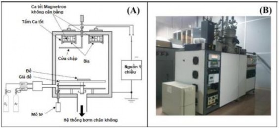
Figure 2.6. (A) Schematic diagram of DC sputtering system; (B) Image of sputtering system at ITIMS Institute.
To modify the surface of SnO 2 nanowires by WO 3 nanoparticles by DC sputtering method, we used W as the target material and SnO 2 nanowires prepared in the first step as the substrate. The DC sputtering power was 50 W, the Ar and O 2 gas flows were 15 sccm and the sputtering times were 36, 60, 120, 240 seconds respectively to create WO 3 nanolayers on the surface of SnO 2 nanowires with estimated thicknesses of 3 nm, 5 nm, 10 nm and 20 nm respectively .
After the sputtering process, the sample was annealed at 600 ºC for 5 hours in air to increase the ability to form the WO 3 structure (tungsten oxide can exist in some other structures such as WO 2 , W 2 O 3 , W 2 O 5 , W 18 O 49 ) and the stability of the contact between WO 3 nanoparticles and SnO 2 nanowires . WO 3 oxide is an n- type semiconductor oxide . Therefore, in the fabricated sensor, a heterojunction layer of the same type of carrier n- SnO 2 /n - WO 3 is formed .
2.3. Method of surveying the structure and morphology of the sensor
The synthesized SnO 2 /SMO heterostructure sensors were morphologically examined by field emission scanning electron microscopy (FESEM, Hitachi S-4800, Japan), high-resolution transmission electron microscopy (HRTEM, Tecnai G2 F20, FEI), selected area electron diffraction (SAED) and elemental composition analysis using an energy-dispersive X-ray spectrometer (EDS) integrated in the electron microscope. These analytical techniques were performed at the Institute of Advanced Science and Technology (AIST) - Hanoi University of Science and Technology and the Vietnam Academy of Science and Technology. The crystal structure of the sample was determined by X-ray diffraction , using characteristic CuK α radiation with a wavelength of 1.54056 Å at a scanning angle of 0.015%. X-ray diffraction analysis was performed on a Bruker D5005 machine at the Faculty of Physics - University of Science - Vietnam National University, Hanoi.
2.4. Method of surveying gas-sensitive characteristics
To evaluate the parameters of a gas sensor that changes conductivity (resistance) in gas environments or in environments with different gas concentrations, the sensor resistance is often measured continuously over time in a background gas environment (usually
air) to the gas medium to be measured. The H 2 S gas sensitivity characteristics of the fabricated sensors were investigated at different temperatures and gas flow rates by dynamic measurement method.
The dynamic measurement method is a method commonly used in research and development of gas sensors. In this method, gas is continuously blown through the measuring chamber and the resistance of the sensor is continuously measured over time. When switching from the background gas state to the measured gas state by a reversing valve, it must be ensured that the flow of gas blown into the measuring chamber is constant (stable pressure). According to this method [1], the concentration of the gas to be measured C (ppm) is determined by the formula:
𝐶 = 𝐶 𝑓
(2.1)
𝑜 𝑓+𝐹
In which f ( sccm), F (sccm) are the standard gas and carrier gas flow rates respectively, C o (ppm) is the standard gas concentration.
Normally, the carrier gas is clean air, which is also the background gas (when compared) in the measurement, and is also the gas diluted into the gas concentrations to be measured [1]. For the dynamic measurement method, the response and recovery time of the sensor is almost independent of the volume of the measuring chamber but depends on the air flow rate through the measuring chamber. In addition, the response and recovery time of the sensor depends on the nature of the gas-sensitive material layer and on the working temperature of the sensor.
The main components of the gas measurement system for the dynamic measurement method at ITIMS Institute (Figure 2.6) include:
- Gas mixing system: uses gas flow controllers to create the gas concentration to be measured.
- Gas measurement chamber: The sample is placed on a heating furnace connected to a temperature controller to create the temperature to be investigated. The maximum temperature of the furnace is 450 o C. The sample is connected to a Keithley 6002 A source and controlled by the Labview program through the probes placed on the electrode feet. In addition, the gas measurement chamber is also connected to a pump to suck the exhaust gas out.
In this study, to generate the measured gas concentrations we used a one-pass gas mixing system with three mass flow controllers (MFCs) as shown in Figure 2.7.
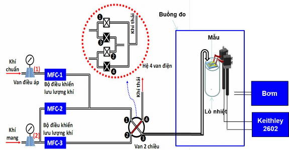
Figure 2.7. Schematic diagram of the gas measurement system for the dynamic measurement method at ITIMS Institute [1].
The MFC-1 controller is used to control the flow rate (f) of the standard gas, the MFC-2 (F) is used to control the flow rate of the carrier gas (usually air) to mix with the standard gas flow. Just changing the gas flow ratio in these two flow controllers will obtain different gas concentrations while ensuring the total gas flow remains constant (Equation 2.1). The MFC-3 is used to control the baseline flow rate of the carrier gas, which has a flow rate equal to the total gas flow rate of MFC-1 and MFC-2. On the other hand, the gas mixing system requires pressure regulators (1) and (2) to stabilize the pressure before and after the MFCs. Furthermore, a 2-way air valve is used to bring air into the measuring chamber. This valve must ensure the following principle: when switching the valve, the air flow from MFC-1 and MFC-2 enters port 1 and exits 3, while the air from MFC-3 enters from port 2 and exits port 4. At this time, the measured air flow enters the measuring chamber and the background air flow goes to the exhaust pipe. When switching to the recovery measurement state, the air from MFC-1 and MFC-2 goes from port 1 and exits port 4 into the exhaust pipe, while the air flow from MFC-3 enters from port 2 and exits port 3. At this time, the background air enters the measuring chamber. In some cases, it is possible to design 4 electric valves as shown in Figure 2.6 in the red dashed circle. These four valves will have two states: valves 1 and 2 are closed while 3 and 4 are open. When switching states, 3 and 4 are closed, while 1 and 2 are open.
2.5. Conclusion of Chapter 2
In chapter 2, the thesis presented the experimental steps in fabricating SnO 2 /SMO heterostructure nanowire sensors and the method of investigating the structural morphology of the fabricated sensors as well as the method of investigating the gas sensitivity of the sensors:
Fabrication of SnO 2 nanowires by thermal evaporation method, with Pt electrode coated with 5 nm thick Au catalyst layer.
Modifying the surface of SnO 2 nanowires by electron beam evaporation with Ni metal for different times combined with thermal annealing in air to create heterostructure nanowires with different types of n- SnO 2 / p- NiO carriers with different NiO coating thicknesses.
Modify the surface of SnO 2 nanowires by dipping SnO 2 nanowires in AgNO 3 salt solution to create heterostructure nanowires with different carrier types n- SnO 2 / p- Ag 2 O with different densities of modified nanoparticles.
Modify the surface of SnO 2 nanowires with ZnO layer by CVD method with the growth time of the modified layer being 5, 10, 15 minutes to create heterostructured nanowires with the same type of n- SnO 2 / n- ZnO carriers with different thickness of the modified layer.
Modify the surface of SnO 2 nanowires by DC sputtering method with different metal targets W and sputtering times combined with annealing in air to create heterostructure nanowires with the same type of n- SnO 2 / n- WO 3 carriers with different thicknesses of modified nanolayers.
Present methods for studying the morphology and structure of the manufactured sensors.
Present the method of investigating the sensitivity of H2S gas of sensors.
CHAPTER 3: RESULTS OF RESEARCH ON FABRICATION AND GAS SENSITIVITY OF SEMICONDUCTOR METAL OXIDE NANOWIRE STRUCTURE n- SnO 2 / p- SMO
In this chapter, we present the results of the study on the fabrication of heterostructured semiconductor metal oxide nanowires with n- SnO 2 / p- SMO carriers and the low concentration H 2 S gas sensitivity characteristics (1 ÷ 10 ppm) of the fabricated samples. The study results also show the influence of the thickness of Ag 2 O, NiO modification layer on the surface of SnO 2 nanowires and the working temperature of the sensor on the gas sensitivity properties. The H 2 S gas sensitivity mechanism of the sensor is explained by the energy band theory and the sulfidation process.
n- SnO 2 / p- Ag 2 O structured nanowire sensor
The structure, chemical composition and structural characteristics of SnO 2 nanowires surface modified by Ag 2 O nanoparticles by CVD method combined with dip coating method were studied by scanning electron microscopy (SEM; JEOL 7600F), and energy dispersive X-ray spectroscopy (EDS), transmission electron microscopy (HRTEM; JEOL 2100F) and X-ray diffraction (XRD; ….) [2]. After morphological and structural testing, the sensors were examined for their sensitivity to H 2 S gas at concentrations of 0.1 ÷ 1 ppm.
3.1.1. Morphology and structure of the sensor
To investigate the morphology, structure and properties of the material, we selected unmodified SnO 2 nanowire sensor samples (S0), the SnO 2 /Ag 2 O structure created corresponding to the SnO 2 nanowire immersed in AgNO 3 salt solution with a concentration of 0.2 mM, 1 immersion (S2) and the SnO 2 /Ag 2 O structure created corresponding to the AgNO 3 salt concentration of 1 mM, 20 immersions (S5) for SEM, EDS and TEM analysis. Figure 3.1 (A) illustrates the SEM image of the SnO 2 nanowire sensor (S0) grown on an Au-coated Pt electrode . Notably, the comb electrode used had a gap distance of 20 μm, the long grown SnO 2 nanowires bridged the gaps between the two electrodes. SnO 2 nanowires grew mainly on the surface of Pt comb electrodes, but the
Their length is controlled enough to connect between the comb teeth and thus act as channels in the gas measurement of the sensor. The average diameter of the nanowires is about 70 nm. The surface of the unmodified SnO 2 nanowires is smooth, with a single-crystal structure . This result is consistent with the nanowire growth by the vapor-liquid-solid mechanism [98]. Here we used gold as a catalyst in the growth of SnO 2 wires , so the belt-like NWs are obtained in the initial state. The SnO 2 nanowires have a single-crystal structure as presented in the article by NXThai et al. [67]. Composition analysis of SnO 2 nanowires by energy dispersive X-ray spectroscopy (EDS) - Figure 3.1 (B) shows the existence of O 2 , Sn and Pt elements where Pt is from the electrode, while O 2 and Sn are from the SnO 2 nanowires .
The SEM images of SnO 2 NWs after being modified by Ag 2 O nanoparticle layer (S2) are shown in Figure 3.1(C), in which the insets are low magnification SEM images. The comb electrodes were covered with SnO 2 NWs, the nanowire surface was coated with Ag 2 O nanoparticles by dip coating method which maintained the morphology of SnO 2 NWs but the nanowire surfaces were not as smooth as the original sample and very small particles were seen in the SEM image. The high magnification SEM image showed the presence of Ag 2 O nanoparticles on the surface of SnO 2 nanowires . EDS analysis of sample S2 - Figure 3.1(D) confirmed the presence of Ag at the energy level of 2.98 eV. The SEM image of sample S5 is shown in Figure 3.1(E). With the increase of AgNO 3 concentration to 1 mM and the number of dip coating times is 20, the morphology of the modified SnO 2 nanowires changes. The surface of the sensors is found to have increased roughness. Ag 2 O nanoparticles can be seen in the SEM image of sample S5. Continuous or discontinuous Ag 2 O nanoparticles are attached on the surface of SnO 2 nanowires . EDS analysis of sample S5 in Figure 3.1(F) shows that the density of Ag is very high (about 3.5wt%). This result demonstrated that increasing the concentration of AgNO 3 salt solution and the number of dip coating times can increase the density of Ag 2 O nanoparticles on the surface of SnO 2 nanowires .
To further study the modification results of Ag 2 O nanoparticles on the surface of SnO 2 nanowires , we selected samples S0, S2 and S5 to observe by transmission electron microscopy (TEM) (Figure 3.2).