formed on the surface. The density and size of the particles depend on factors such as: gold concentration in the solution, electrolysis time, or stirring conditions. The formation of different morphologies of the Au-NP layer will have a decisive influence on the sensitivity of the fabricated electrode. is an SEM image
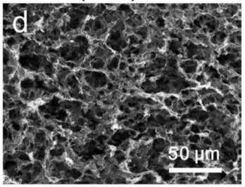
Figure 1. 9. SEM image of graphene fabricated by CVD method [98].
Figure 1.9 is an SEM image of graphene prepared by chemical vapor deposition ( CVD ) [98]. The obtained image shows that graphene has a porous honeycomb structure. With this structure, the material has a large working surface area and high adsorption capacity. The authors have successfully used the material in the analysis and detection of heavy metals.
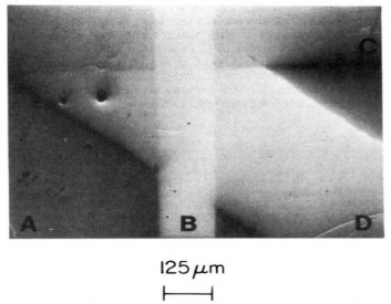
Figure 1. 10. SEM image of SAM fabricated by the templating method. Region A: Au substrate. Region B: dibutylamine. Region C: diethanolamine. Region D: HN(C10H21)- (C8H2F15) [99]
SEM method was also used by author Eric W. Wollman when evaluating the quality of image transmission studying the surface structure of gold electrodes modified by self-assembled monolayer mixture of dibutylamine, diethanolamine and HN(C 10 H 21 )- (C 8 H 2 F 15 ) using 3-keV and 2-nA energy [99]. The regions of different monolayers are shown in Figure 1. 10.
In 2016, author Pham Khac Duy and his colleagues used this method to study the tree-shaped porous gold nanostructure fabricated by the static flow method on carbon fabric (CFC-AuNDs) (Figure 1.11) [100]. SEM images show that the formed gold layer has a three-dimensional tree-shaped porous form with nanometer size. The research team also confirmed that the three-dimensional tree-shaped porous structure significantly increases the active area and catalytic activity of the electrode and has been successfully applied in the analysis of Hg(II) with ppb-sized amounts.
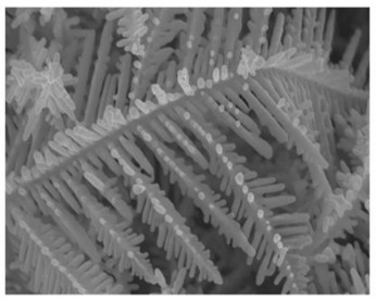
Figure 1. 11. SEM image of CFC-AuNDs prepared by the static current method with a time of 240 s [ 100]
1.1.6.2. Transmission electron microscopy (TEM)

Figure 1. 12. TEM method model
Transmission Electron Microscope is a device for studying the microstructure of solid objects, using a high-energy electron beam to penetrate a thin solid specimen and using magnetic lenses to create images with high magnification (up to millions of times), the image is created on a fluorescent membrane or on optical film or digital device.
Transmission electron microscopy images are images of the lower surface of the sample obtained by an electron beam passing through the sample, so TEM has better resolution than SEM. TEM plays an important role in the study of small-sized samples [95], allowing the determination of the size, morphology, and structure of materials by analyzing the incident electron beam passing through the sample surface.
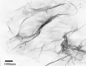
Figure 1. 13. TEM image of graphene [101]
When taking pictures of nano-sized samples, the resolution of the transmission electron microscope is good (0.1nm), with that resolution enough to observe nano-sized details. When preparing the sample for shooting, the sample must be made very thin (half a micrometer) so that electrons can penetrate the sample to create a magnified image. When the sample is thin without distorting the structure, the transmission electron microscope can reveal many nano-details of the research sample such as the shape, size of the particles, and the composition of the substances.
Recently, the group of authors Yuli Wei and colleagues [101] used the TEM method to study the structure of graphene (Figure 1.13). The results showed that the graphene sheet has a transparent and wrinkled thin film structure. The author also explained that this is an important factor that increases the elasticity of the two-dimensional crystal to reduce the disturbance caused by thermal deformation and keep the material stable.
1.1.6.3. FTIR infrared spectroscopy method
Infrared spectroscopy is based on the interaction of light rays in the infrared region (400 – 4000 cm -1 ) with bonds in the molecules of the substance under study. Light rays with certain wavelengths will cause certain bonds to vibrate. Therefore, the corresponding energy absorption is closely related to the molecular structure.
There are two main vibrations: stretching vibration and bending vibration. When infrared radiation is irradiated on a molecule, photons with energy equal to the difference in energy between vibrational energy levels in the molecule will be absorbed and we obtain an infrared spectrum (IR).
Based on the characteristic frequency and peak intensity in the infrared spectrum, the presence of bonds and functional groups in the studied molecule can be determined, thereby determining the structure of the studied substance. Infrared spectroscopy is used for both qualitative and quantitative analysis.
In the study of nanostructures, infrared spectroscopy is an effective method used to study the structure of modified materials. For example, the author group Rotake. DR (2020) used the FTIR method to study the structure of Homocysteine on the Au/Ti platform with different modification methods. The sensor after fabrication was analyzed for Hg (II) with a detection limit of 27.42 ng/mL [102].
1.1.6.4. Cyclic voltammetry method
Cyclic voltammetry is one of the most effective and widely used measurement techniques in the study of electrochemical properties as well as the kinetics and reaction mechanisms of the studied substance on different electrodes. The essence of this technique is potentiodynamic, which is the potential being swept linearly over time. However, after a certain period of time, , the potential sweep direction is reversed at the potential E . Therefore , the potential applied to the static electrode has a triangular waveform as illustrated in Figure 1.14a. During the potential sweep, the electrochemical device measures the current obtained from the electrode reaction, the dependence iE obtained is as shown in Figure 1.14b (characteristic peak i p at which the maximum current corresponds to the potential E p ).
(a)
(b)
Figure 1. 14. Principle of cyclic voltammetry over time and cyclic voltammetry spectrum In the study of the structure of nanomaterials, cyclic voltammetry technique is
used to detect the presence and study the electrochemical properties of materials.
modification on the surface of the electrode. Electrochemically active materials will form oxidation or reduction peaks, or both, in the cyclic voltammetry spectrum. The peak position will reflect the electrochemical reaction energy and is characteristic of each substance. By this measurement technique, it is possible to determine the individual reduction step of the reactant, the potential range at which the electrochemical reaction takes place, the value E p, and the corresponding current density value i p . The electrochemical reaction of the analytes participating (oxidized) in the forward scan direction and the products formed (reduced) in the reverse scan direction, can be represented by the following equation:
Oxidation + ne Reduction (1.2)
An example of this technique is shown in Figure 1.15. Yun Wu and colleagues studied the coverage of the adsorbed SAM layer through the electrochemical value of the reduction peaks. The research group used the CV scanning method to examine the electrochemical signal of 2,5 Dimercapto 1,3,4 thiadiazole (DMTD) on a gold electrode. The adsorption of DMTD on the electrode covered the gold surface, limiting the charge transfer process, causing the electrochemical signal in the Fe(CN) 6 3- / Fe(CN) 6 2- solution to decrease and the distance between the anode peak and the cathode peak to increase sharply (Figure 1.15). The absorption of DMDT on a gold electrode has been successfully applied by the author in the analysis of Pb2+ ions[103]
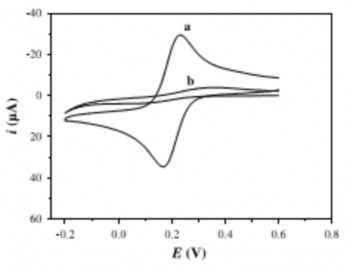
CV curves of gold electrode (a) and DMTD/Au electrode (b) in Fe(CN) 6 3- / Fe(CN) 6 2- solution [103 ]
In 2014, the research group of Thiers Massami Uehara [104] investigated the effect of immersion time of gold electrodes modified by C16SH by CV scanning method in Fe(CN) 6 3- / Fe(CN) 6 2- solution (Figure 1.16). The results showed that the longer the immersion time of SAM, the more the electrochemical signal decreased because some defective areas of the surface were filled by C16SH, leading to covering the gold surface.
CV curves of different immersion times of gold electrode modified by C16SH at 1mM concentration in Fe(CN) 6 3- / solution
Fe(CN) 6 2- [ 104]
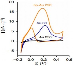
Figure 1. 17. CV curves of 250nm and 30 nm sized AuNPs in 0.5 M KOH solution [ 105] |
Maybe you are interested!
-

 Research on the treatment of seafood wastewater by electrocoagulation method combined with USBF - 19 tank
 -
 Revenue Forecast of Nam Viet Corporation 2014 Using Brown Method
 -
 Equivalent Annual Payment Method
 -
 Summary of Sem Linear Structural Model Data
 -
 Teaching Process of Science Subject Using Btnb Method
In 2014, the group of authors Srikanth Pedireddy [105] used the CV method to detect the presence of AuNPs at different particle sizes. Figure 1.17 shows
The peak peaks at 0.16 V and 0.2 V correspond to the oxidation potential of gold particles of 30 nm and 250 nm size, respectively.
Through the above studies on structural research methods in the process of creating SAM, we can see the diversity of research methods. Depending on the specific characteristics of the material and the specific research purpose, the appropriate research method is selected.
1.2. Substrate materials used to fabricate self-assembled organic monolayers (SAMs)
SAM is formed when the interaction between the substrate material and the SAM-forming substance occurs during adsorption. If the electrode surface is modified with a nanostructured material, the surface area will increase significantly compared to the unmodified electrode. As a result, the measured Faraday current will increase significantly compared to the electrode material without a nanostructure. Therefore, nanostructured materials have been and are being studied for use in the field of electrochemical analysis because the sensitivity of the analysis will be significantly improved. Among the materials used to create nanostructures, metallic gold will be of most interest due to its special physicochemical properties. Therefore, the research in this thesis will focus on the nanostructured substrate material, which is gold nanoparticles (AuNPs) and its composite with graphene oxide (AuNP-GO). These materials are fabricated on a glass carbon electrode (GCE) base to be modified with SAM for application in the analysis of Hg(II) detection in water samples.
1.2.1. Gold nanoparticle material
Nano gold materials have been studied and used in many different fields: electrochemistry [106] , anti-oxidation [107] , medicine [108] , ... because of their outstanding advantages such as: strong adsorption capacity, strong surface plasmon resonance, high surface/volume ratio, particle size ranging from 1-100nm and good electrical conductivity [109], quite different from solid gold materials with disadvantages: high cost, electrode surface needs to be carefully polished to achieve repeatability. In particular, nano gold materials are easily surface modified by adsorbing organic substances to manufacture probes with distinct advantages: lower cost than solid gold electrodes, high stability and repeatability, increased surface active area leading to increased interaction between organic substances and AuNPs.
Therefore, there are three main methods for synthesizing gold nanoparticles: radiation method, chemical reduction method, and electrochemical method.
The radiation method uses UV rays [110], microwaves [111], gamma radiation,... to reduce Au (III) to Au 0 in the presence of suitable stabilizers. This method has the advantage of high synthesis efficiency but the manufacturing equipment is expensive and the machine operation process is complicated.
The chemical reduction method uses a reducing agent to reduce Au (III) in solution to Au 0 . This method has the advantage of creating well-dispersed gold nanoparticles, the resulting particles are small in size, but the manufacturing process requires strict control of influencing factors such as temperature, concentration, pH, etc. [112]. In particular, the chemical method uses reducing agents such as sodium citrate [113], NaBH 4 [114] , ... which are all toxic substances that affect the environment. To overcome this problem, scientists have studied the use of a "green method" using non-toxic chemicals as agents to synthesize typical gold nanoparticles that are widely present in nature, such as chitosan [115]. Chitosan is a bioactive polymer used as a reducing agent in the synthesis of nano gold, with a structure containing a large amount of free amino and hydroxyl groups in the chain, giving it special physicochemical properties such as complexation, film formation and polycation properties. However, chitosan has a disadvantage: it is soluble in acid but not in water or neutral environments, which limits the usability of nano gold.
The electrochemical method for synthesizing gold nanoparticles is used by using an electric current to reduce Au(III) to Au0 on the surface of a solid electrode, for example a glassy carbon electrode (GCE). When using this method, the surface treatment of the substrate electrode, stirring speed, and electrolysis time are important conditions. Therefore, the values of these parameters need to be studied to achieve suitable particle size and density. This method has many advantages such as good quality, simple equipment, low cost, and easy control of the size and distribution of particles on the substrate electrode by electrochemical techniques with different electrolysis conditions [116].
Surface morphology of GCE-modified AuNP electrodes deposited by fixed voltage [117] and cyclic voltammetry [118], or AuNPs generated on fiber sheets